
About SUNWIN
Shenzhen Sunwin Electronics Technology Co., Ltd. provides precision electronics manufacturing services. Our focus includes optical transceiver PCBA, MEMS optical device packaging and sensor modules. We help customers move from development builds to volume production.
SUNWIN is the overseas business company of Saketron Electronics, our shareholder and manufacturing base. Established in 2009, the manufacturing base has more than 15 years of experience in electronics manufacturing services (EMS). Its work covers optical communication, wearables, RF and radar systems, fingerprint security and automotive sensing.
The manufacturing base is a National High-Tech Enterprise and a recognized specialized and innovative enterprise. It was also included in Shenzhen's first batch of Advanced Smart Factories for 2026.
We serve more than 50 customers in optical communication, including over 10 publicly listed companies. Our manufacturing support combines precision processes, production capacity and digital quality control.
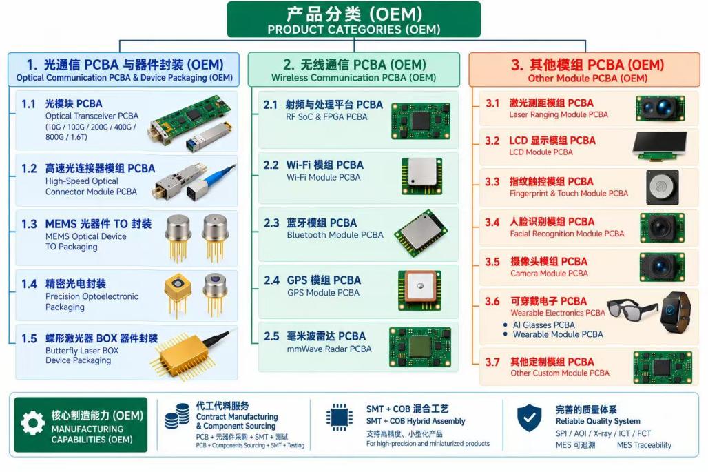
Three core manufacturing services
Our manufacturing base has more than 8,000 square metres of cleanroom production space across five floors. It operates 21 SMT lines and two chip-on-board (COB) packaging workshops. Equipment includes systems from Yamaha, K&S, FT and Vitronics Soltec.
Capabilities include 01005 component placement, flip-chip assembly and hermetic TO packaging. These processes support three core service areas.
Optical transceiver PCBA
We manufacture PCBA for optical transceivers from 10G to 1.6T. We also assemble RF boards and other wireless communication products. This supports customers working across both optical and wireless applications.
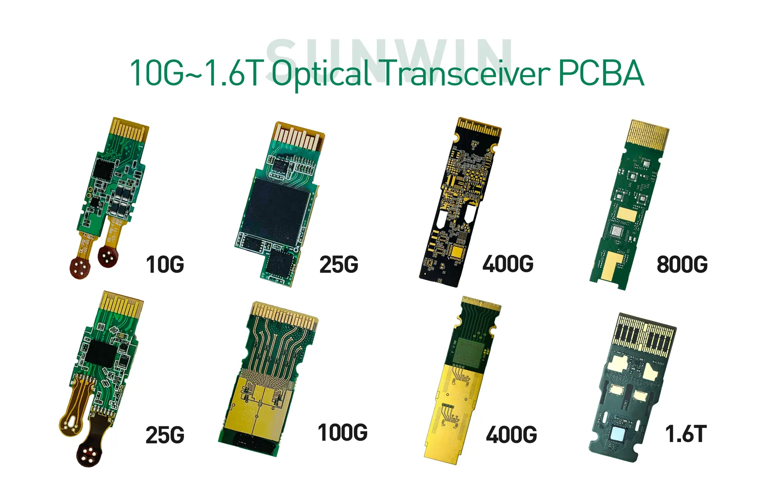
Examples of optical transceiver PCBA from 10G to 1.6T.
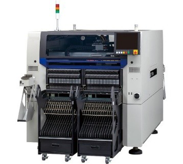
High-speed dual-beam placement machine.
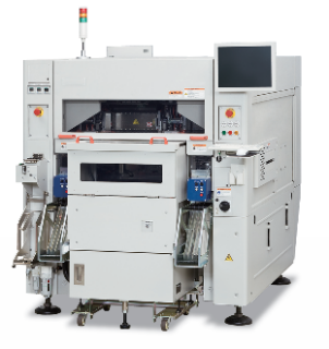
Flip-chip placement machine.
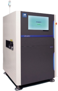
3D automated optical inspection (AOI).
MEMS optical device TO packaging
We provide TO packaging for MEMS optical switches, MEMS variable optical attenuators (VOAs) and other optoelectronic devices. Supported formats include TO-38, TO-46, TO-56 and TO-60.
The process covers die attach, silver paste application, gold wire bonding, lens micro-assembly and hermetic cap sealing.
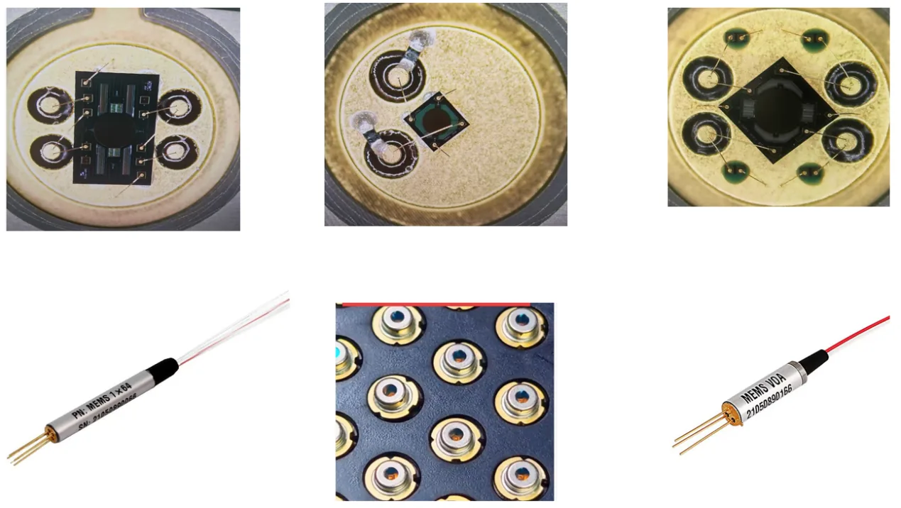
Examples of MEMS optical switch and MEMS VOA TO packaging.
Sensor module manufacturing and packaging
We manufacture and package sensors and sensor modules for automotive sensing, industrial detection and related applications. The manufacturing base holds IATF 16949 certification for its automotive quality management system.
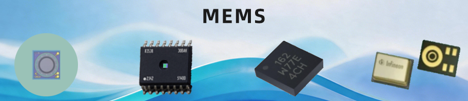
Examples of packaged MEMS sensors.
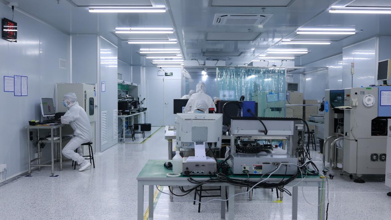
Packaging workshop at the manufacturing base.
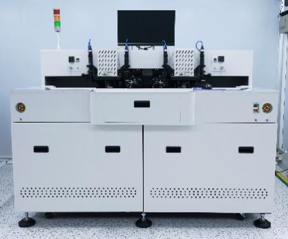
Automatic high-speed die bonder.
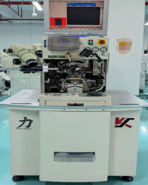
Automatic gold wire bonder.
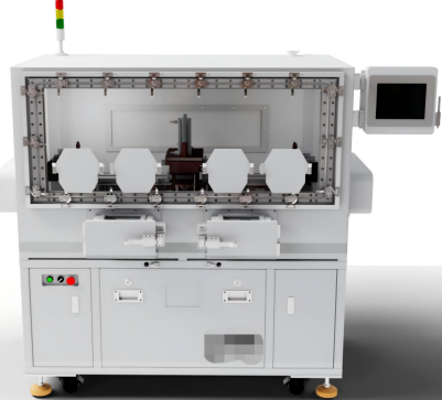
Automatic cap sealer.
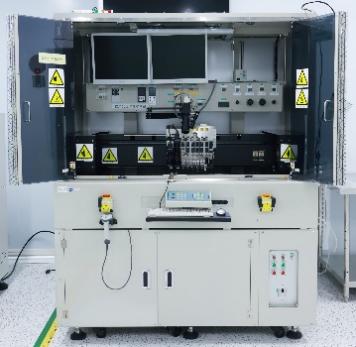
Micron-precision eutectic bonder.
Precision processes for volume production
Our technical team works on the manufacturing challenges behind compact, highly integrated products. Capabilities include:
- Ultra-small component placement, including 008004 components measuring 0.2 × 0.1 mm.
- Flip-chip and wafer attachment.
- Precision soldering for CoC/CoS, WLCSP and SiP assemblies.
- Optical microlens assembly.
- Combined SMT and COB processes.
- 2.5D and 3D stacking processes.
Process controls address common defects such as poor solder joints, tombstoning, solder voids, adhesive residue and component cracking. The aim is consistent quality as products move into volume production.
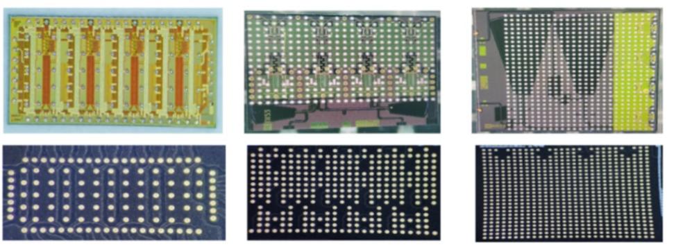
Flip-chip capability: minimum bump pitch of 110 μm and bump diameter of at least 60 μm.
For optoelectronic packaging, dedicated Class 100 clean workstations support standardized assembly procedures. Controls focus on silver paste bubbles, package cracks, hermetic leaks and scratches on optical lenses. These measures support the reliability of optical chips, lasers and photodetectors.
Production capacity and flexible delivery
The manufacturing base has a daily placement capacity of more than 30 million components. Monthly capacity reaches 800 million placements. It can also produce more than 150,000 MEMS optical TO assemblies per month.
A flexible production system supports both small development batches and volume orders. A rapid-prototyping service is available around the clock. This helps coordinate pilot builds, production schedules and capacity allocation.
Direct access to factory production lines reduces intermediate steps. Quotes are transparent, with no hidden charges.
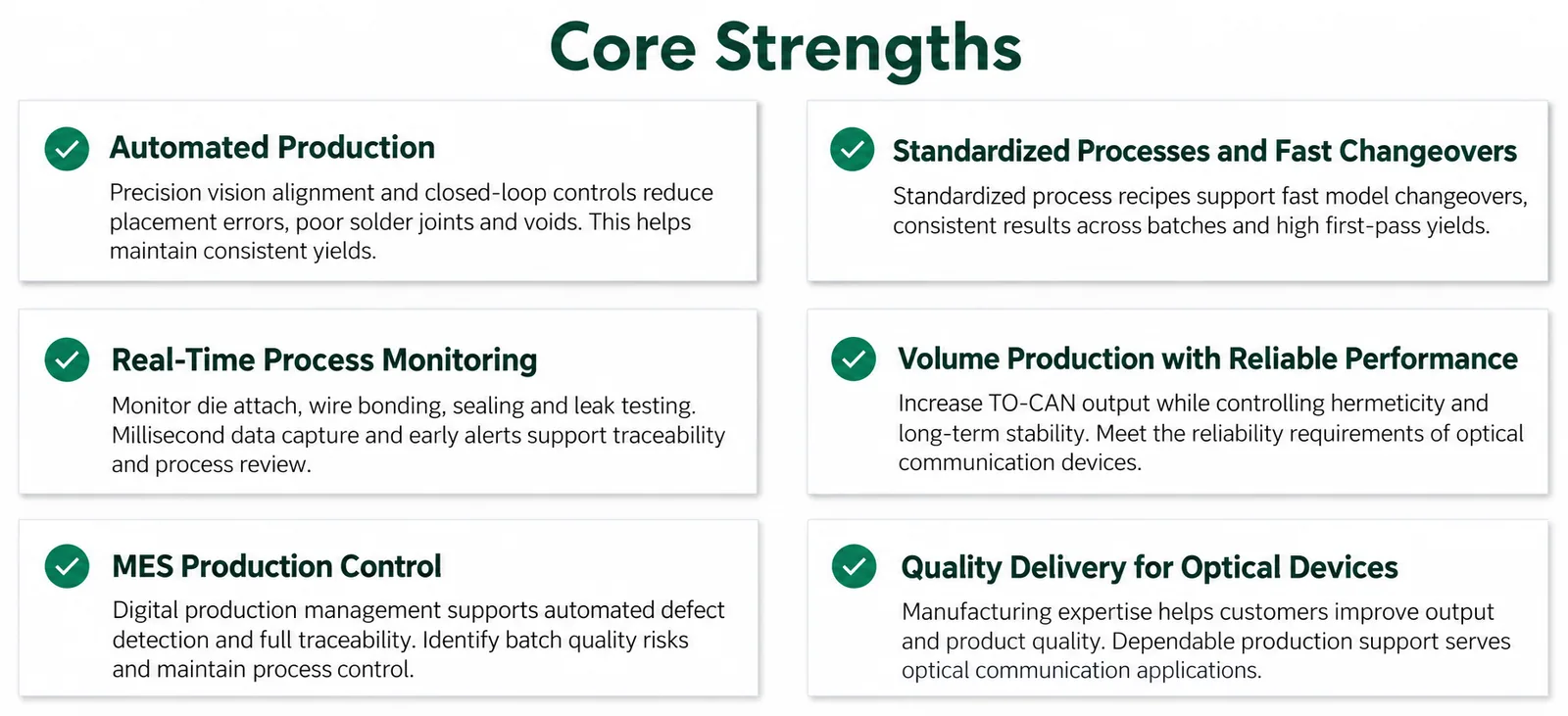
Quality systems and traceability
The manufacturing base holds ISO 9001, ISO 14001, IATF 16949 and QC 080000 certifications. A manufacturing execution system (MES) and Kingdee ERP support traceability across materials, production steps, inspections and batches. These records also support customer supply-chain audits.
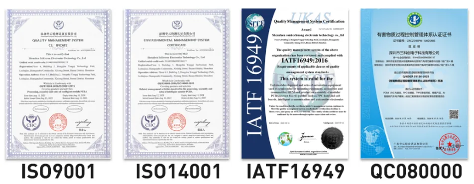
Certifications held by the manufacturing base. The certificates retain the original certified entity's name.
Supporting optical communication and sensing applications
AI data centres, smart vehicles and smart factories are expanding the use of optical communication devices and MEMS sensors. Higher integration and reliability requirements place greater demands on manufacturing and packaging.
Precision PCBA, hermetic TO packaging and sensor micro-assembly all affect product performance, yield and production consistency. SUNWIN combines these services to support customers facing assembly defects, packaging leaks, unstable yields, delivery delays or limited traceability.
Contact SUNWIN
To discuss optical transceiver PCBA, MEMS TO packaging or a custom sensor module project, contact Mr. Dai.
- Phone / WhatsApp / WeChat: +86 185 7660 1365
- Address: 2nd Floor, Building A, Hongzhu Yongqi Science and Technology Park, Hangcheng Street, Bao'an District, Shenzhen, Guangdong, China.
- Website: sunwinmodules.com