
Sunwin's flagship product line — PCBA manufacturing and precision packaging for optical modules and devices.
PCBA manufacturing and precision device packaging for optical communication, from 10G to 1.6T transceiver boards to hermetic MEMS TO and butterfly BOX packages.
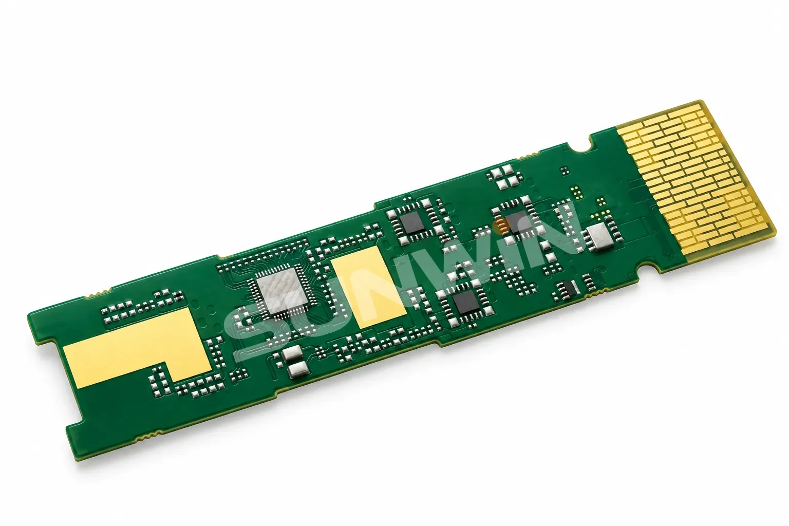
Sunwin manufactures optical transceiver PCBAs from 10G to 1.6T, combining 01005 placement, flip-chip assembly down to 110 μm bump pitch and hybrid SMT + COB processes. Every board passes 100% SPI, 3D AOI and full CCD inspection, with lot-level MES traceability from incoming material to shipment.
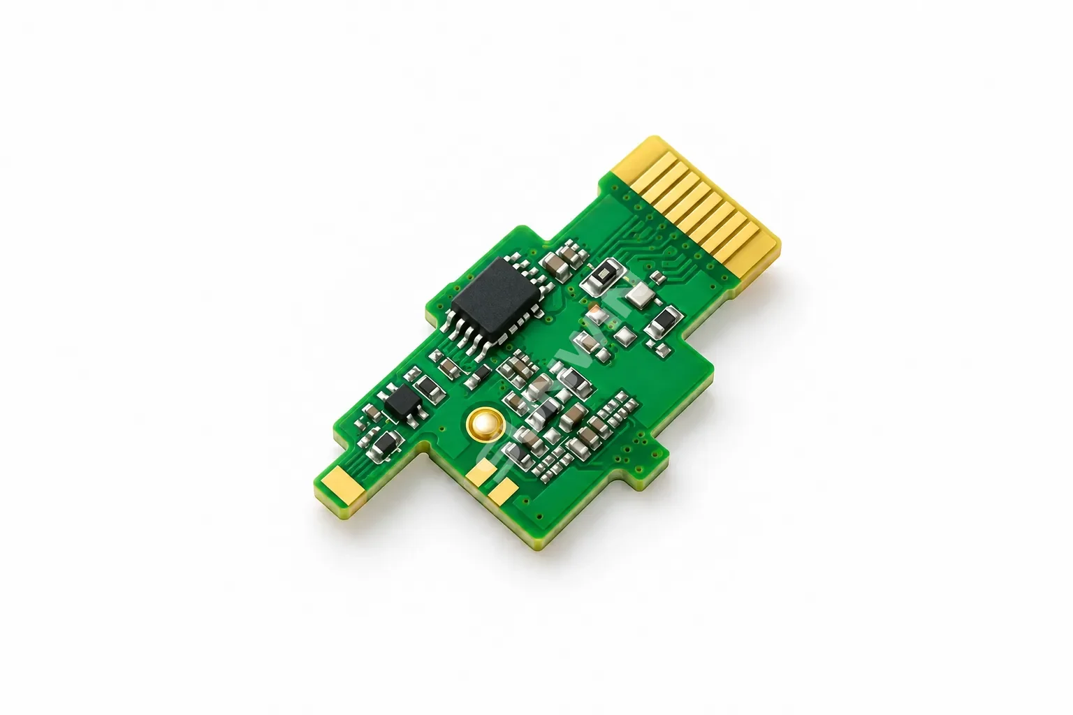
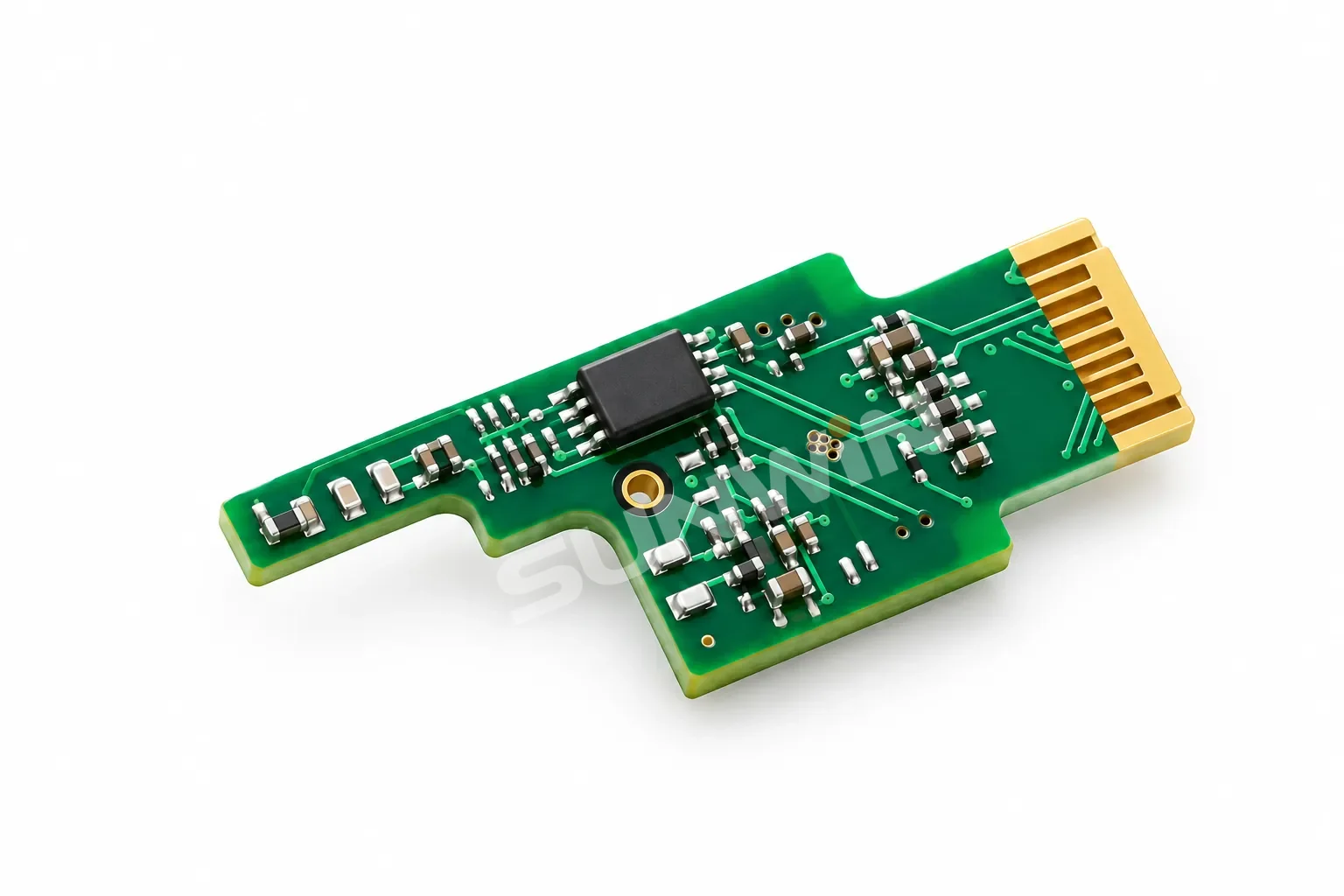
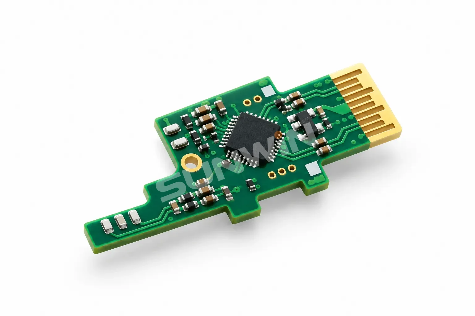
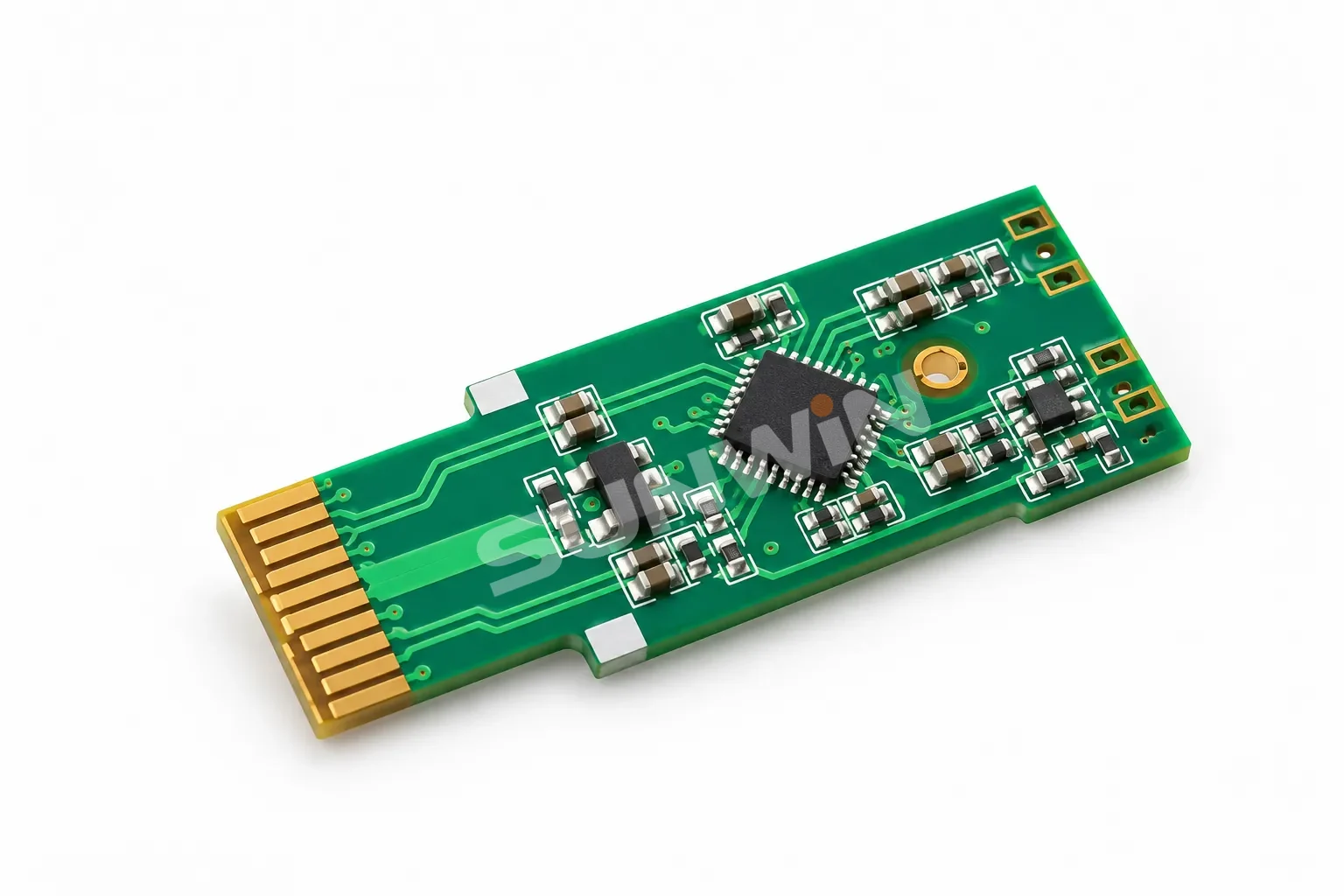
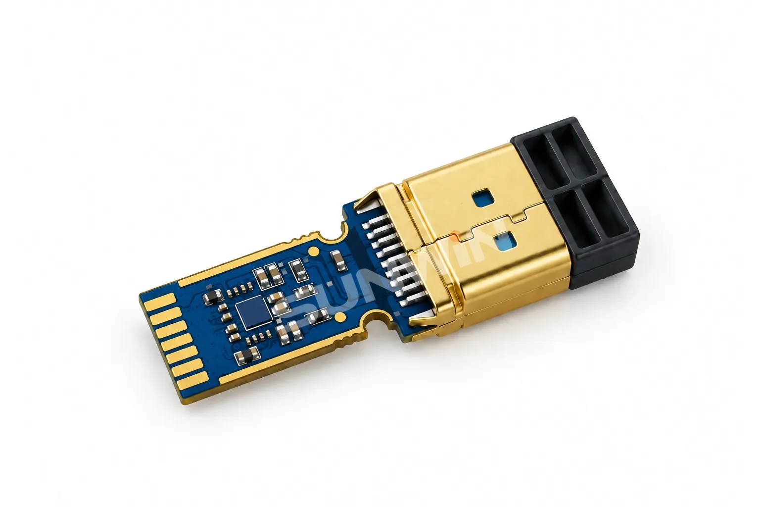
Sunwin assembles PCBAs for high-speed optical connector modules on the same SMT + COB platform used for transceiver boards, with dedicated fixtures and inspection for dual-row connectors, fine-pitch parts and gold-finger areas.
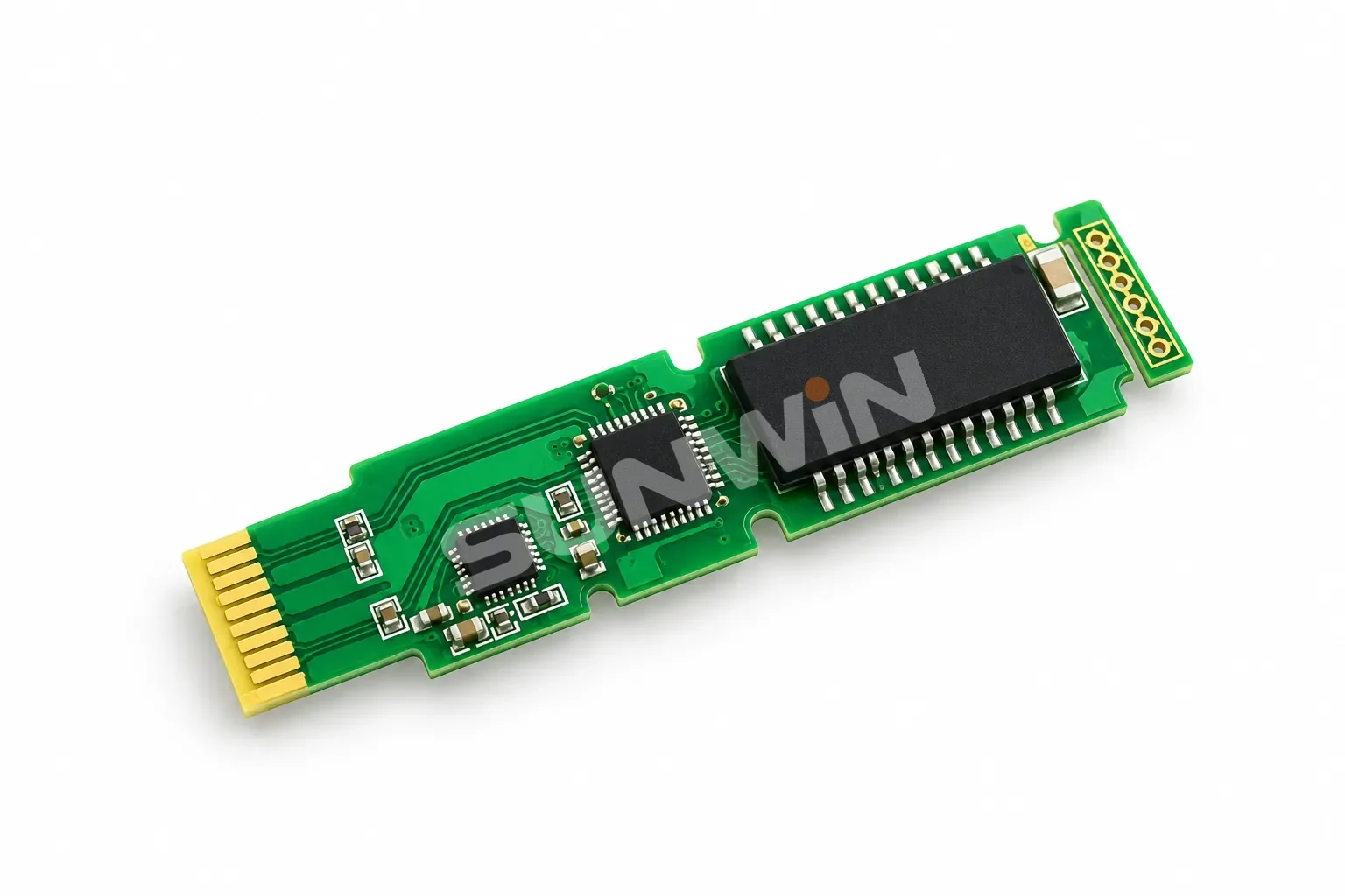
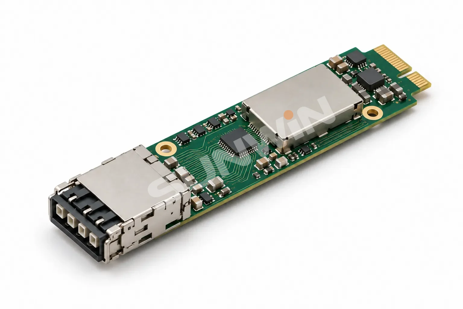
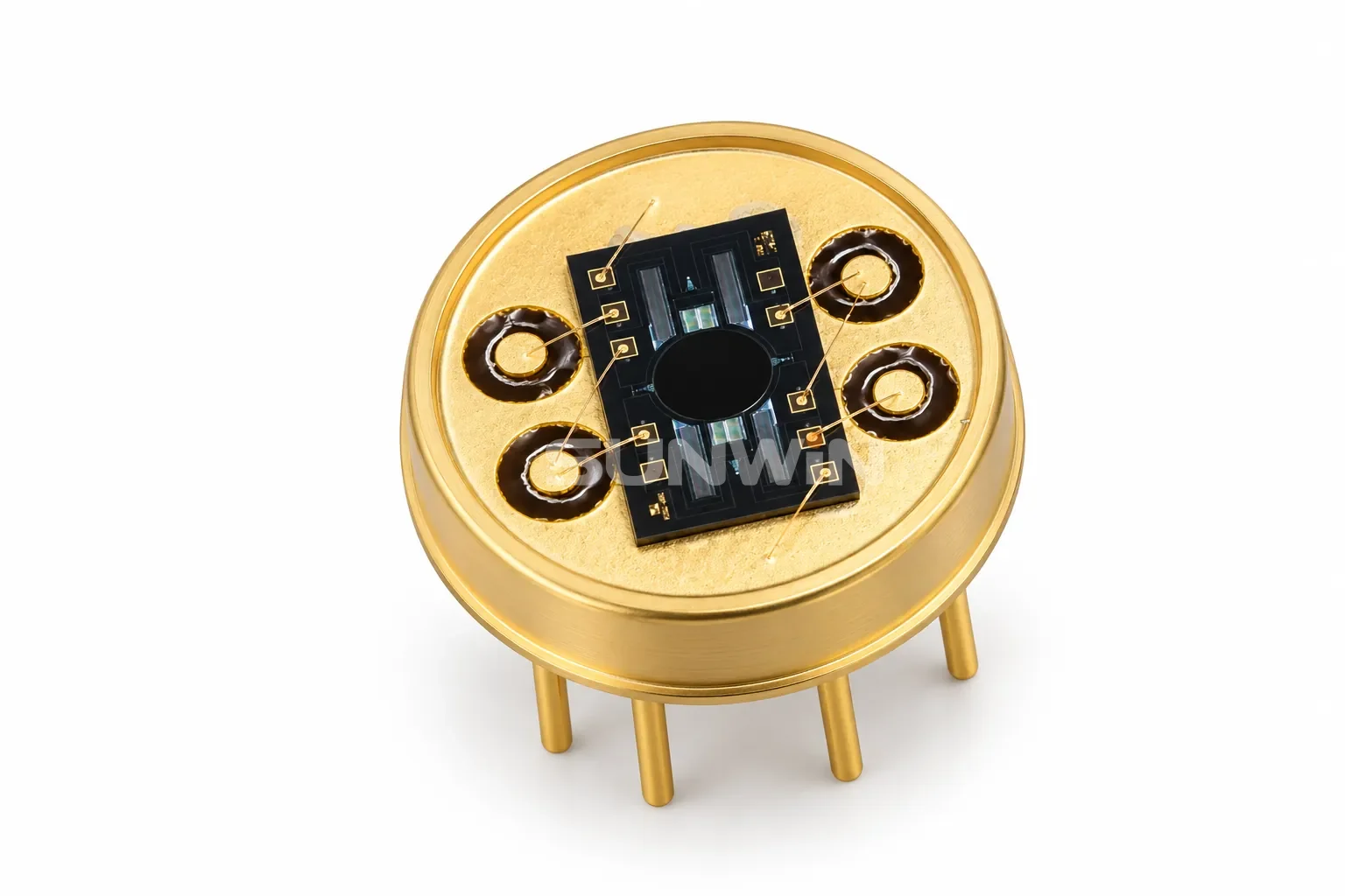
Sunwin provides hermetic Kovar TO packaging for MEMS optical switches, MEMS variable optical attenuators (VOA), lasers and photodetectors in TO-38, TO-46, TO-56 and TO-60 formats. Packaging runs in Class 10,000 cleanrooms with Class 100 control at critical steps, with capacity above 150,000 MEMS optical TO assemblies per month.
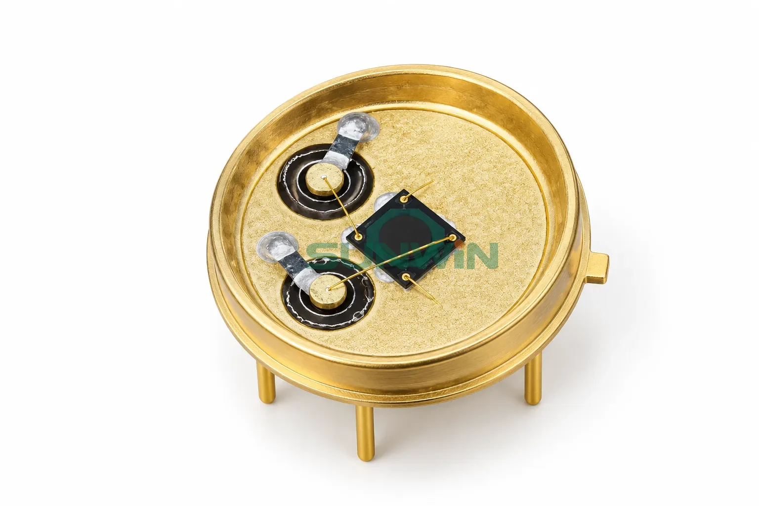
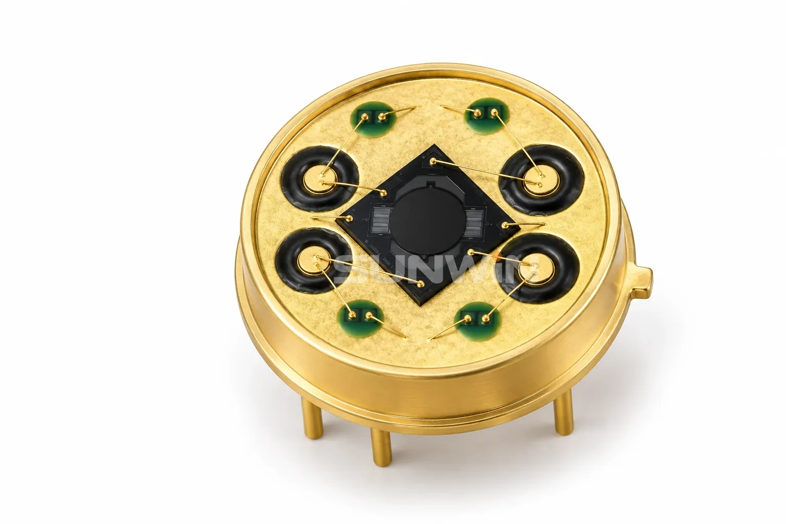
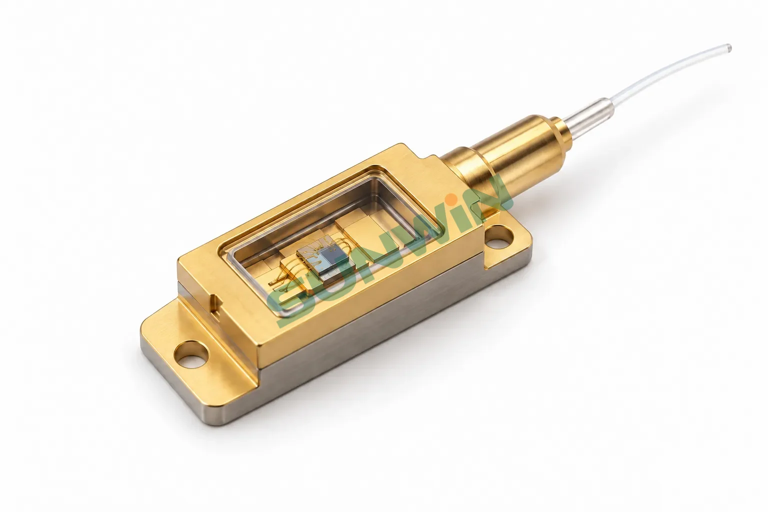
Sunwin packages small, dense optoelectronic modules and devices using COB and hybrid SMT + COB processes: laser and photodiode die attach, TIA, driver and DSP assembly, CoC and CoS builds, micro-lens and isolator placement, and MEMS sensor packaging.
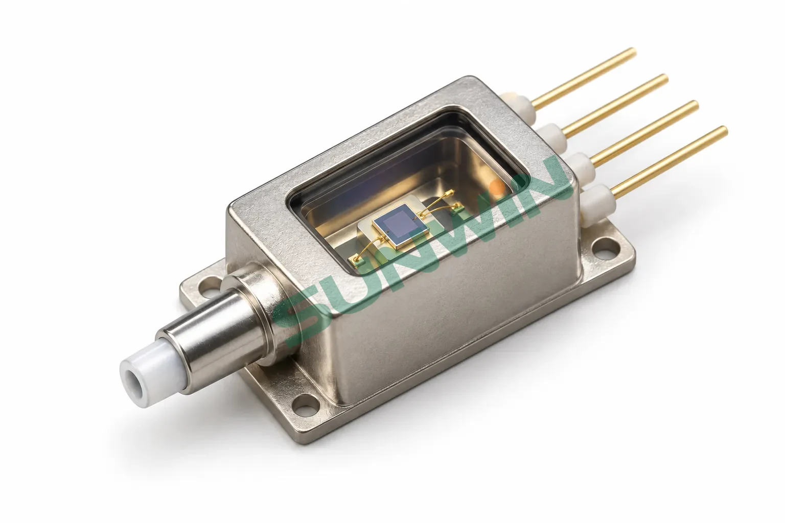
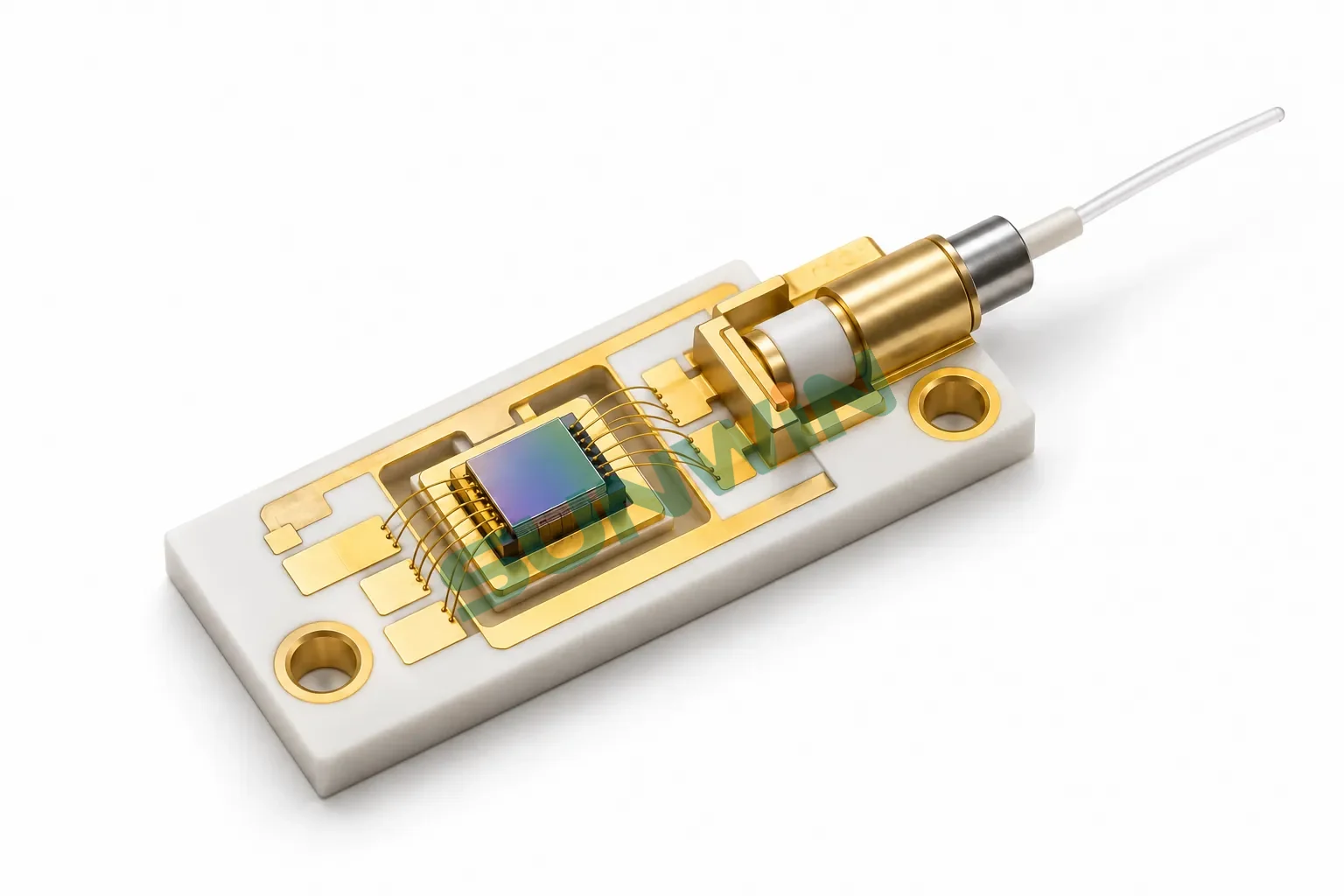
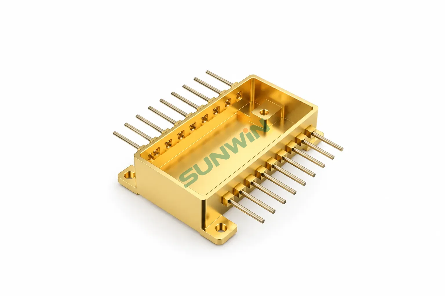
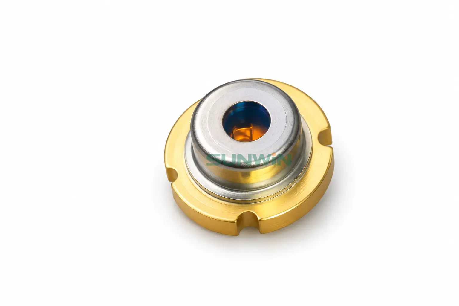
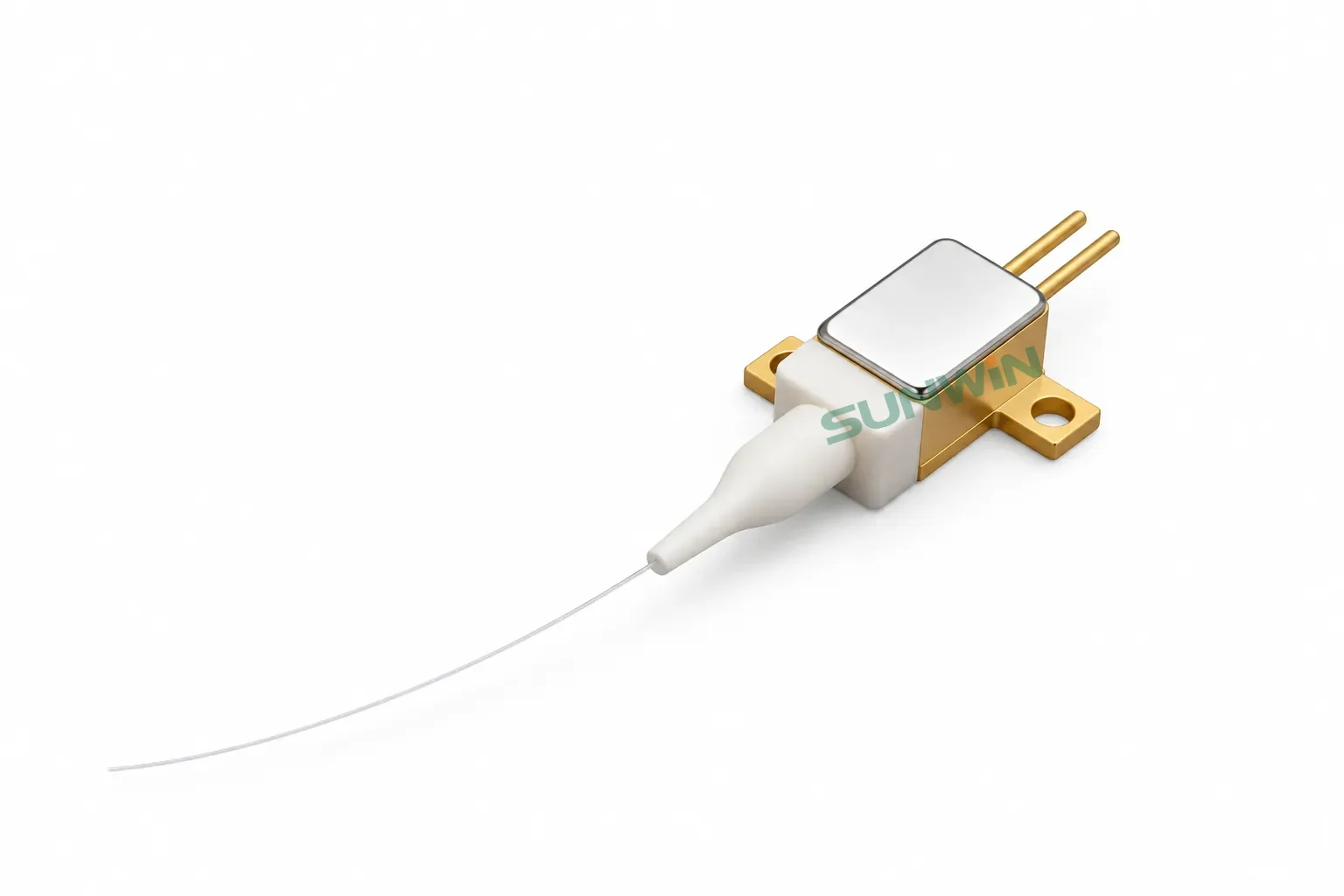
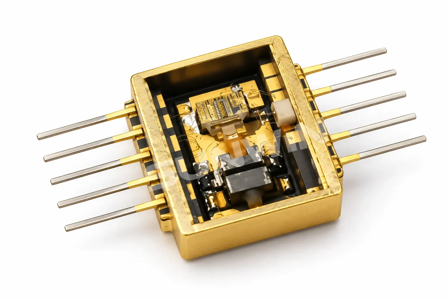
Sunwin packages lasers and optoelectronic devices in butterfly and BOX housings: die attach and wire bonding inside metal or ceramic housings, optical subassembly placement and alignment, lid seam welding and helium leak testing.
Tell us your module type and specs — we can evaluate a custom PCBA manufacturing solution.

Scan with WeChat to add us