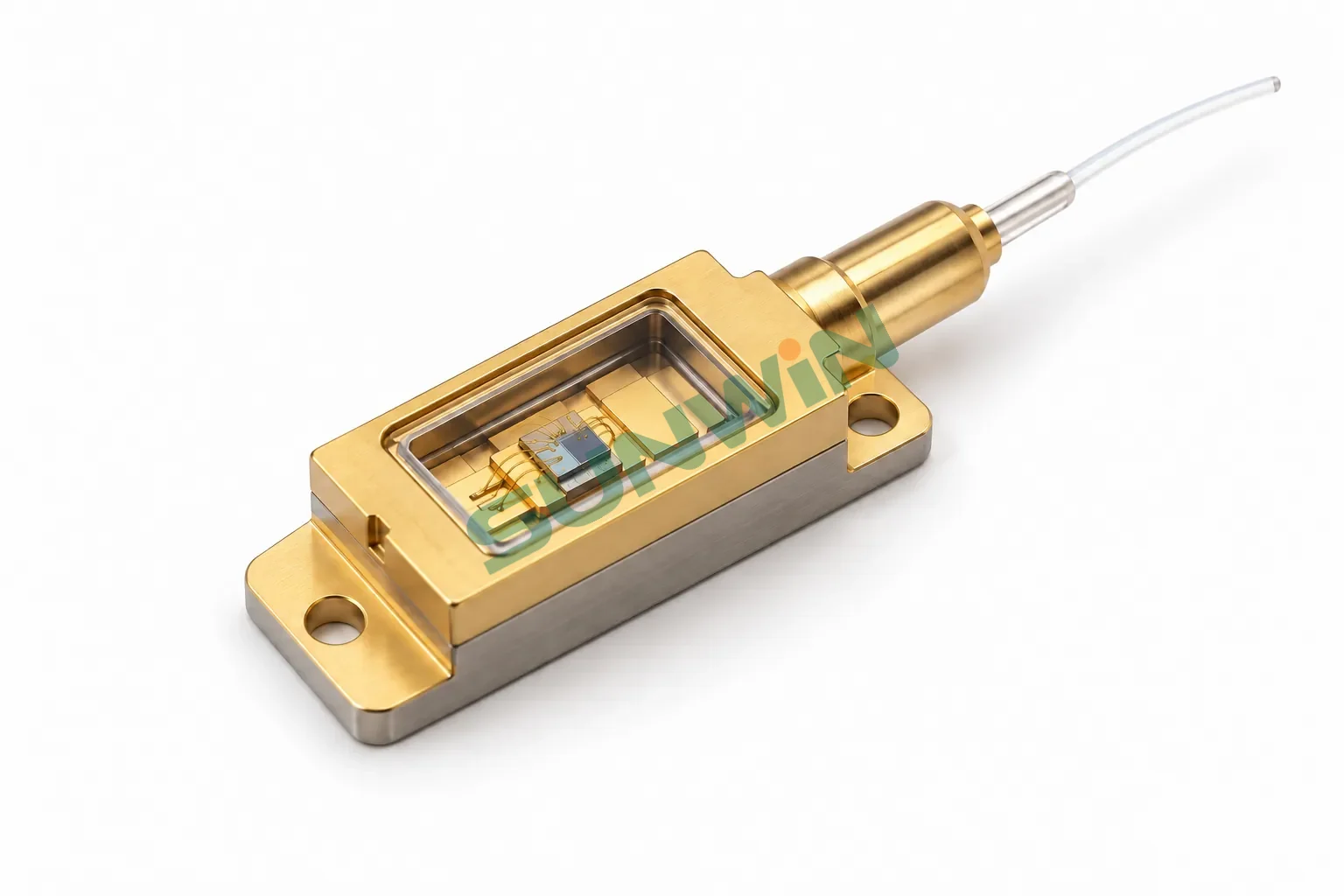
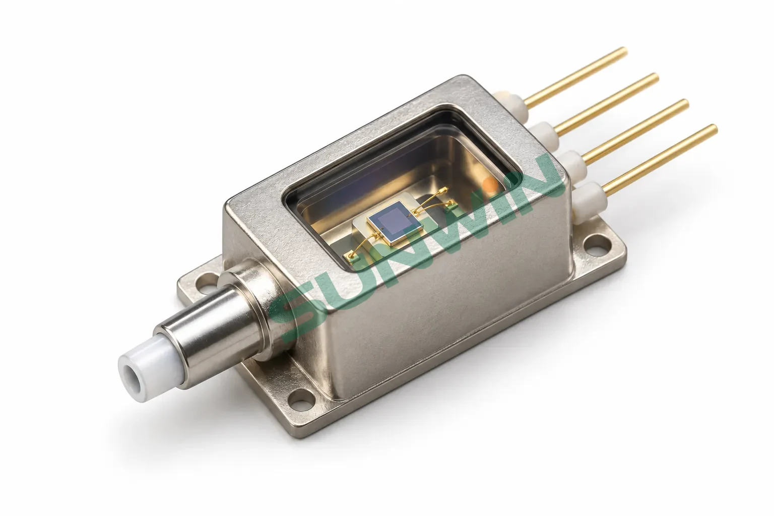
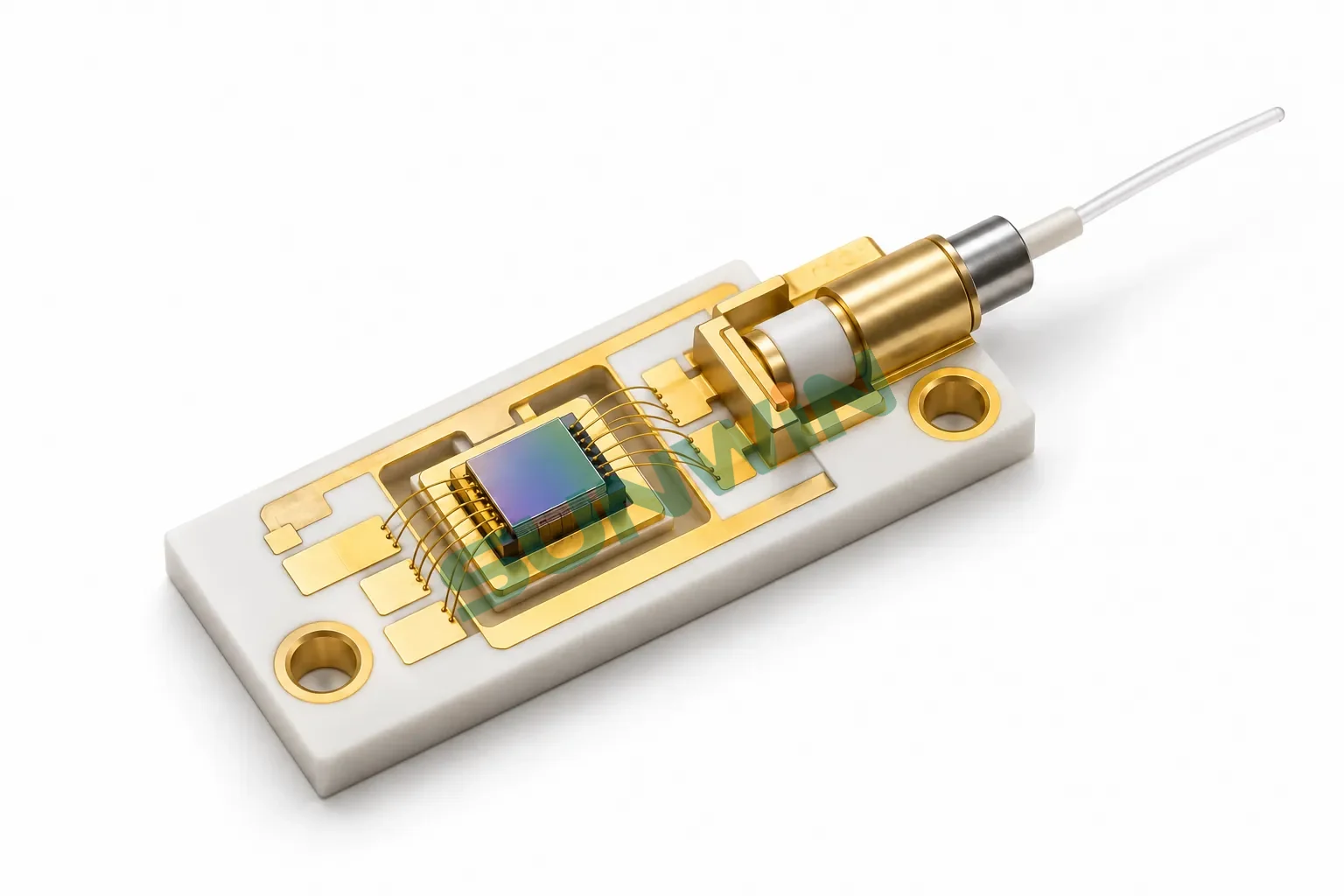
Sunwin packages small, dense optoelectronic modules and devices using COB and hybrid SMT + COB processes: laser and photodiode die attach, TIA, driver and DSP assembly, CoC and CoS builds, micro-lens and isolator placement, and MEMS sensor packaging.
sunwin@saketron.com · sunwin@thankgain.com · WhatsApp +86-18576601365
| Optical die attach | VCSEL, DFB and EML lasers; PD and APD detectors; driver, TIA and DSP dies — silver epoxy or eutectic bonding |
|---|---|
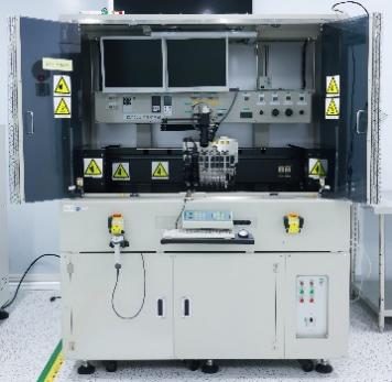
| COB die bond | X/Y ±7 μm, 50–300 mm wafer or waffle-pack feed, 0–360° bond head rotation, 30–150 g bond force |
| Wire bonding | 0.7–1.2 mil wire, ball bonding, plasma pre-clean, pull and shear sampling |
| Optical micro-assembly | Micro-lenses, lens caps, filter caps and optical isolators, with control of orientation, alignment, adhesive volume and cure |
| Chip-level and stacking | CoC, CoS, PoP and 3D stacking with combined flip-chip, die bond and wire bond |
| Sensors and detectors | MEMS gyroscope, microphone and pressure sensor packaging for automotive sensing and industrial detection |
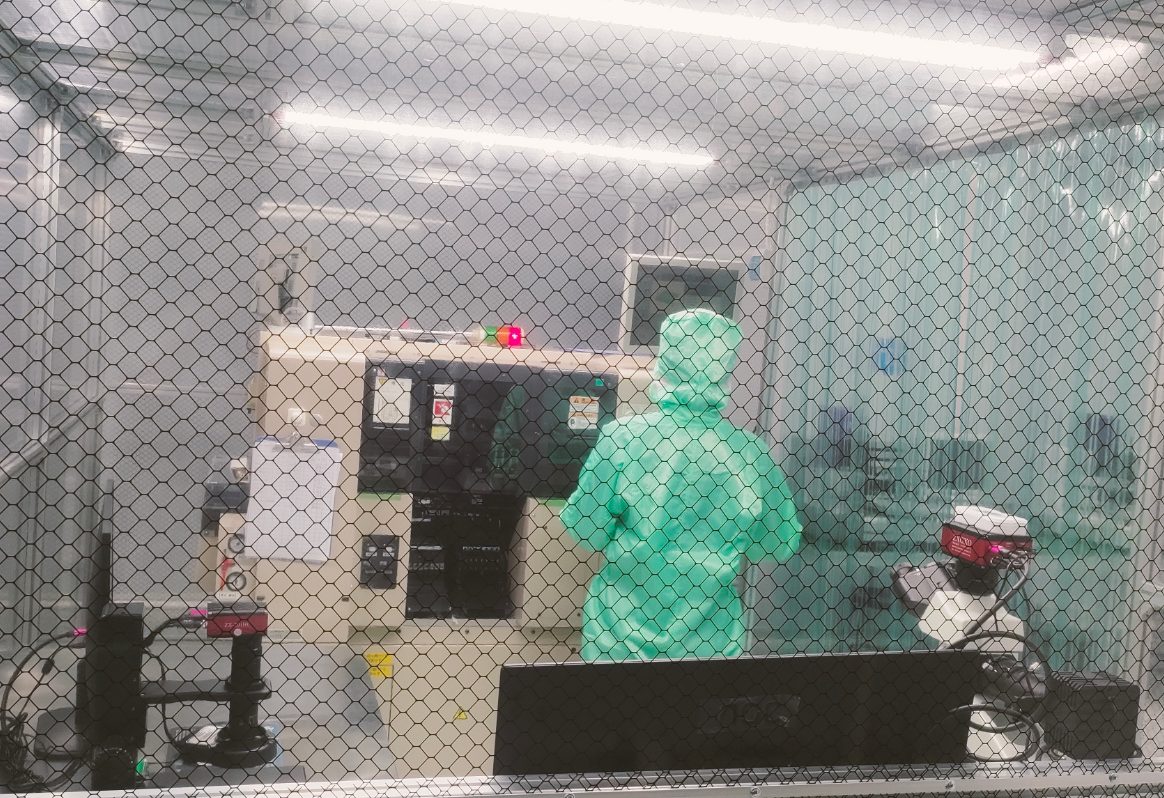
Example assemblies from our production lines.
Yes. Both platforms are available; the choice depends on the die, thermal path and reliability requirement.
Yes, including lens-to-cap assembly, filter caps and optical isolators, with alignment, adhesive volume and cure controlled for each part.
Die and package drawings, bill of materials, process or alignment requirements, reliability specification and forecast volume.
Sunwin is the overseas business company of Shenzhen Saketron Electronics Technology Co., Ltd., its shareholder and manufacturing base since 2009. 21 SMT lines · 8,000+ m². Factory certifications
To start an evaluation, send your Gerber or drawing files, BOM, package or assembly specification, test and quality requirements, and forecast volume.

Scan with WeChat to add us