
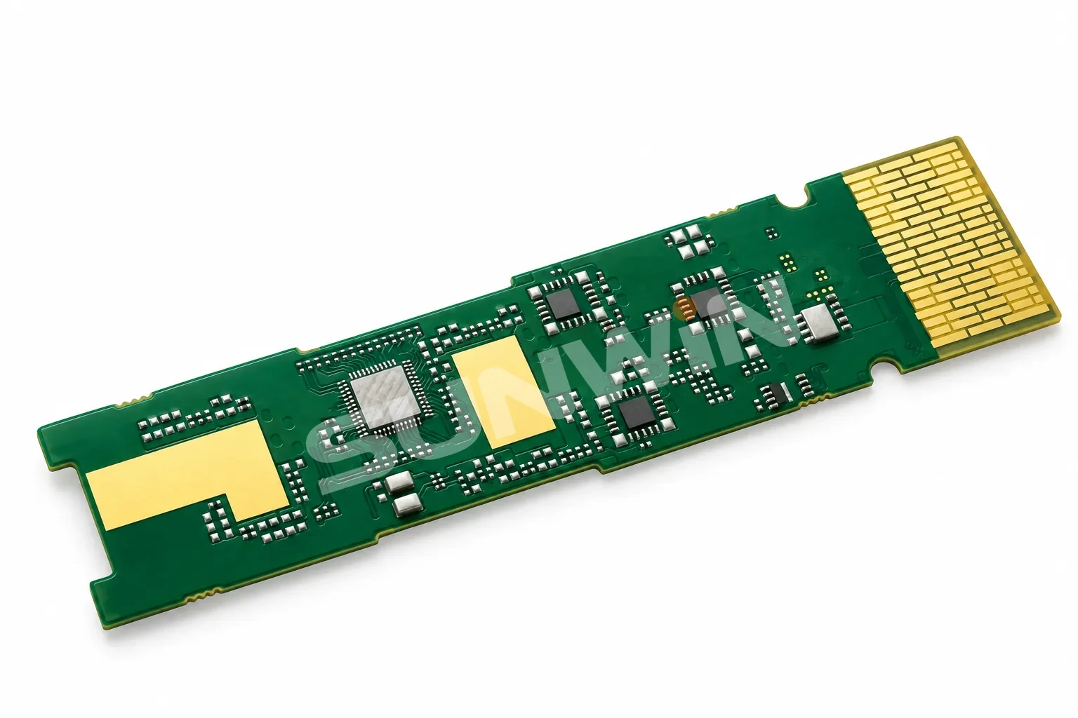
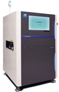
Sunwin manufactures optical transceiver PCBAs from 10G to 1.6T, combining 01005 placement, flip-chip assembly down to 110 μm bump pitch and hybrid SMT + COB processes. Every board passes 100% SPI, 3D AOI and full CCD inspection, with lot-level MES traceability from incoming material to shipment.
sunwin@saketron.com · sunwin@thankgain.com · WhatsApp +86-18576601365
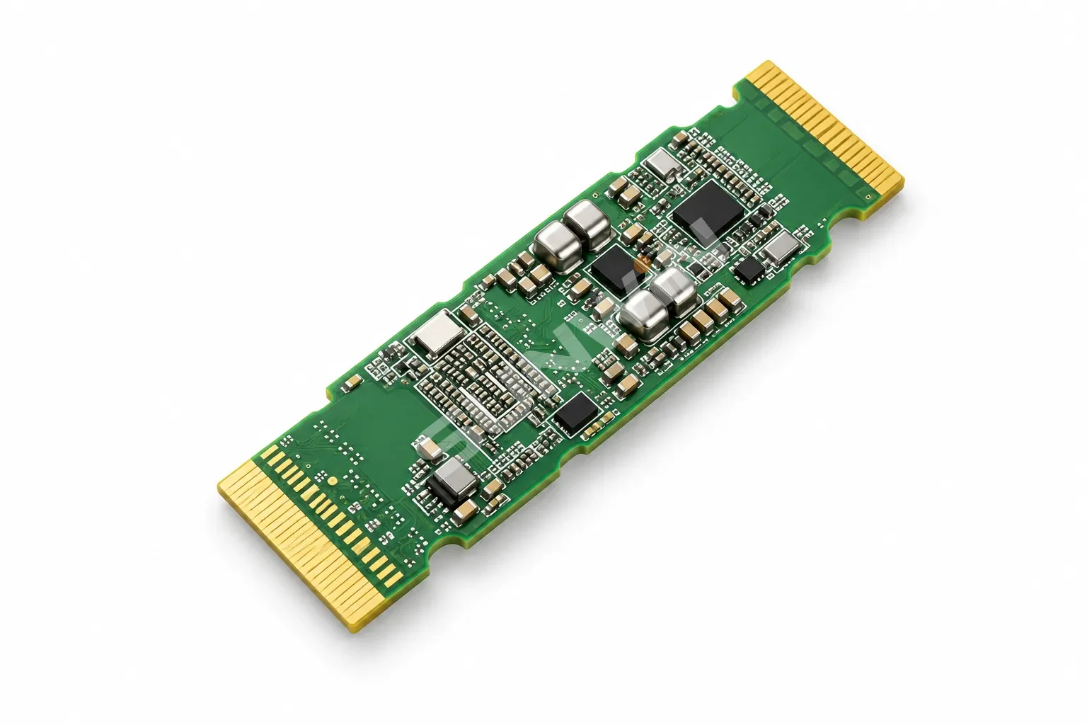
Transceiver boards combine compact layouts, ultra-miniature passives and mixed SMT, COB and bare-die assembly on the same PCB. Our production covers 2.5G, 10G, 25G, 100G, 400G and 800G boards in SFP, SFP+, SFP28, XFP, QSFP28, QSFP-DD and OSFP form factors, with process capability extending to 1.6T platforms.
The manufacturing focus is miniature placement, fine-pitch soldering, protection of COB and gold-finger areas, and complete inspection before release.
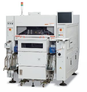
| Miniature components | 008004 (metric 0201), 01005 and 0201; 01005 first-pass yield 99.99% |
|---|---|
| Fine-pitch devices | Minimum pitch 0.15 mm (leaded) / 0.11 mm (ball); BGA/LGA down to 0.35 mm pitch |
| Flip-chip | Minimum bump pitch 110 μm, minimum bump diameter 60 μm; first-pass yield above 98% in volume production |
| System-in-package | PoP and CoC die stacking, SiP and MCP; combined flip-chip, die bond and wire bond flows |
| Special processes | FoB, THR + SMT, wafer and bare-die placement, underfill, conformal coating, 3D assembly |
| Silicon capacitors / CuW | Silicon capacitors 0.6 × 0.3 × 0.15 mm; CuW heat-sink blocks to the customer's die-bond design |
| Substrates | FR4, high-Tg FR4, HDI, FPC, rigid-flex, ceramic and glass |
| Printing | Printing first-pass yield 99.95%; stencils down to 0.04 mm with 0.05 × 0.05 mm apertures; Type 4–7 solder paste |
| Reflow | Nitrogen reflow with oxygen ≤500 ppm |
| PCB size | 50 × 50 mm to 700 × 460 mm |
| Challenge | How we control it |
|---|---|
| Gold-finger solder and COB contamination | Protective tape on COB and gold areas, automated taping and controlled cleaning |
| Solder balls | Paste selection, pad and aperture design, print cleaning, placement force and reflow soak control |
| 01005 placement | Dedicated feeders and nozzles, 3D SPI, aperture design and Type 5 paste |
| LGA/BGA reliability | Baking, pad and stencil design, 3D SPI and placement within ±25 μm |
| Dual-row connectors | Side-push and flatness fixtures, joint volume control and coplanarity checks |
| Board warpage | High-Tg laminate, balanced copper, controlled ramp rates and aluminium support fixtures |
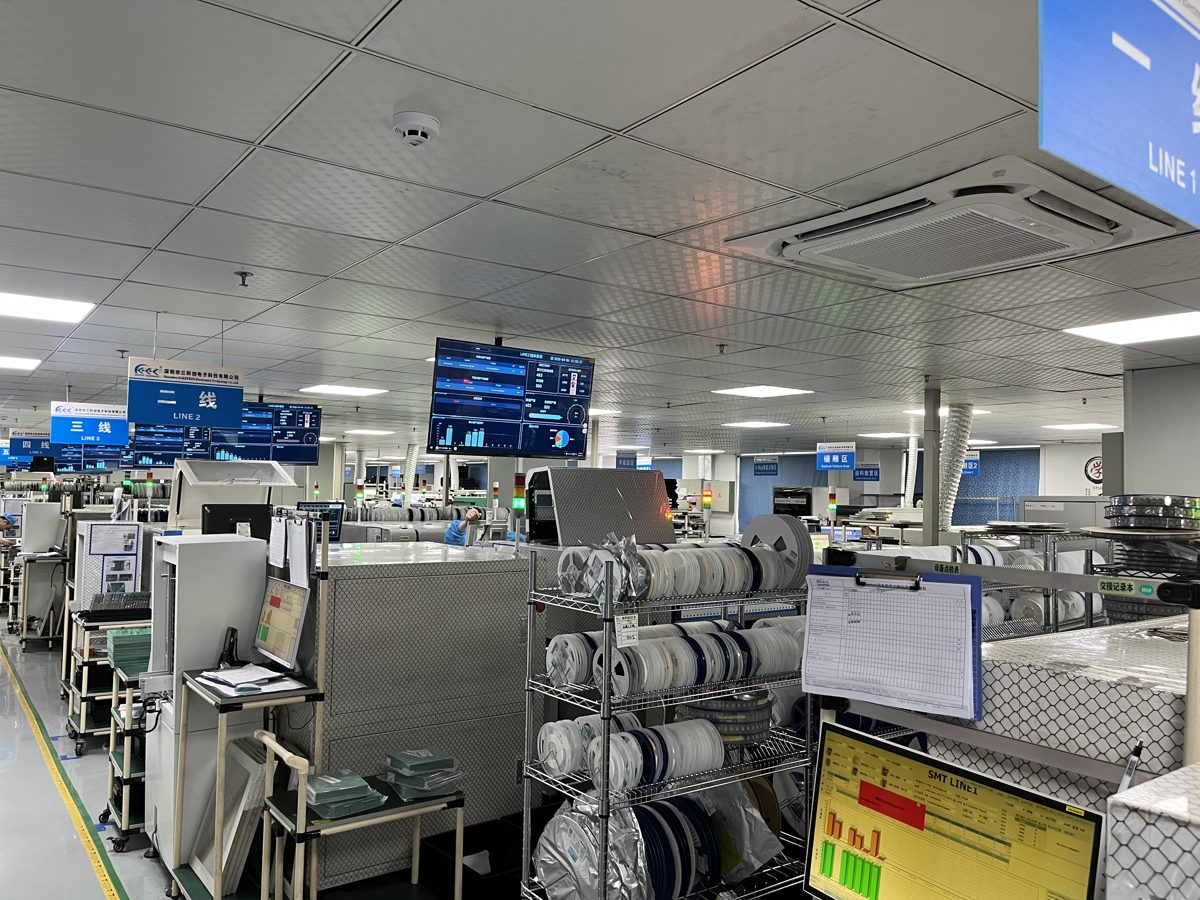
Example assemblies from our production lines.
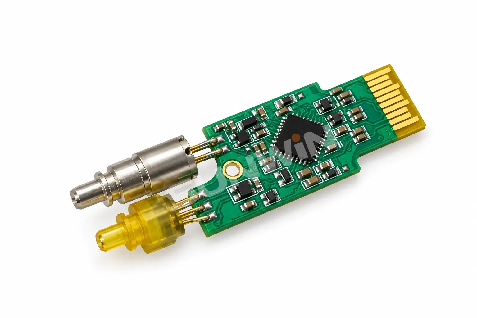
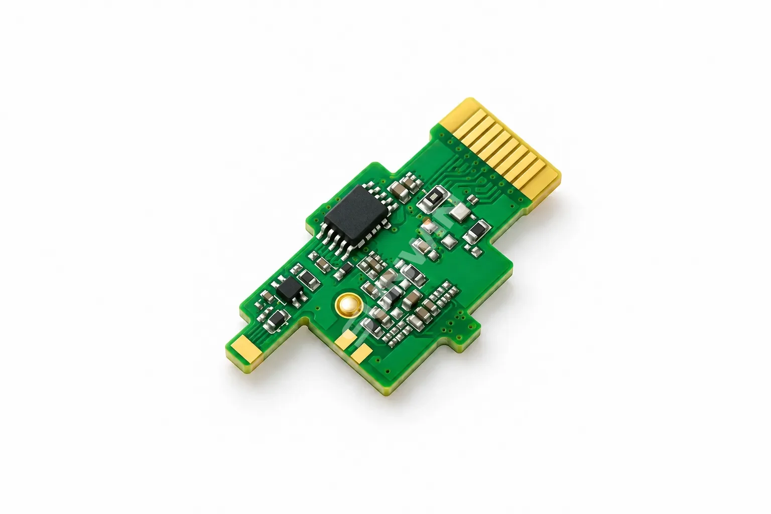
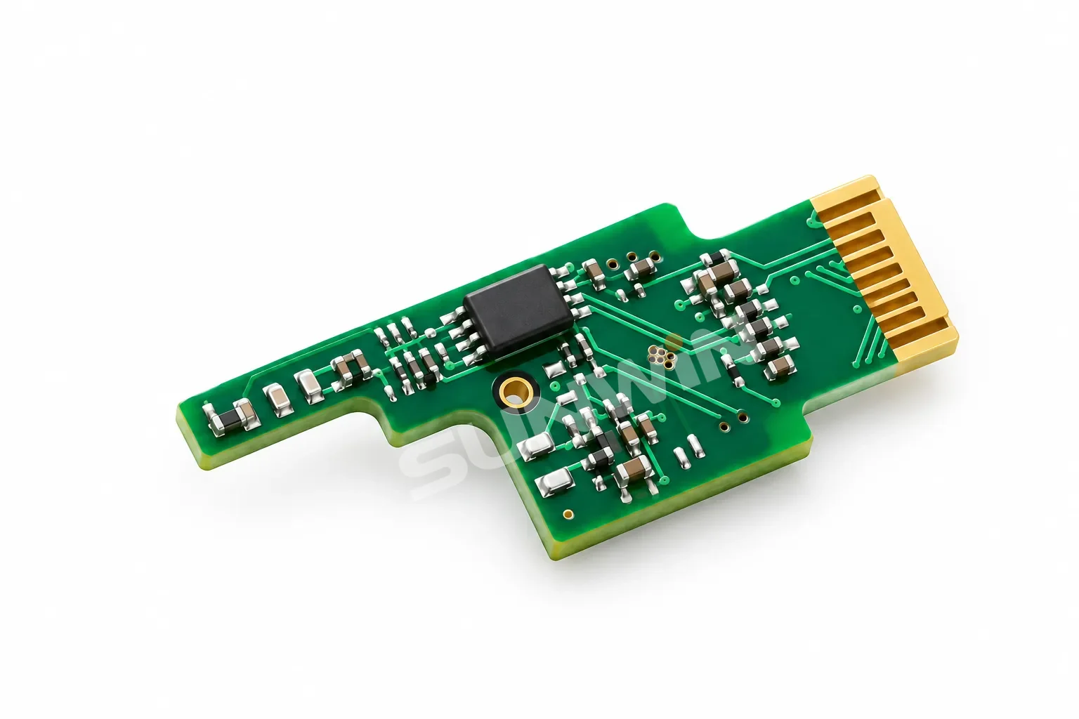
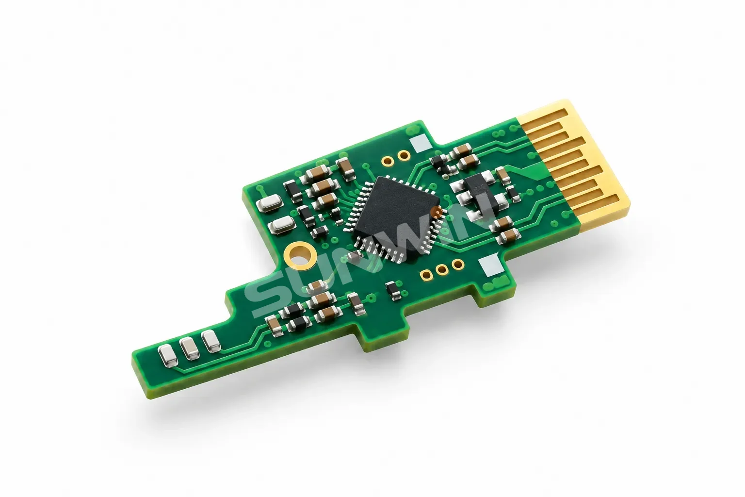
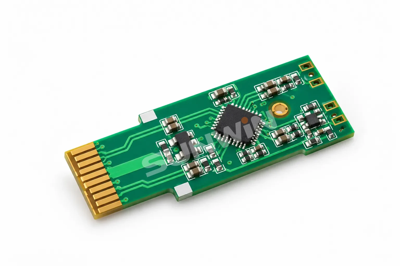
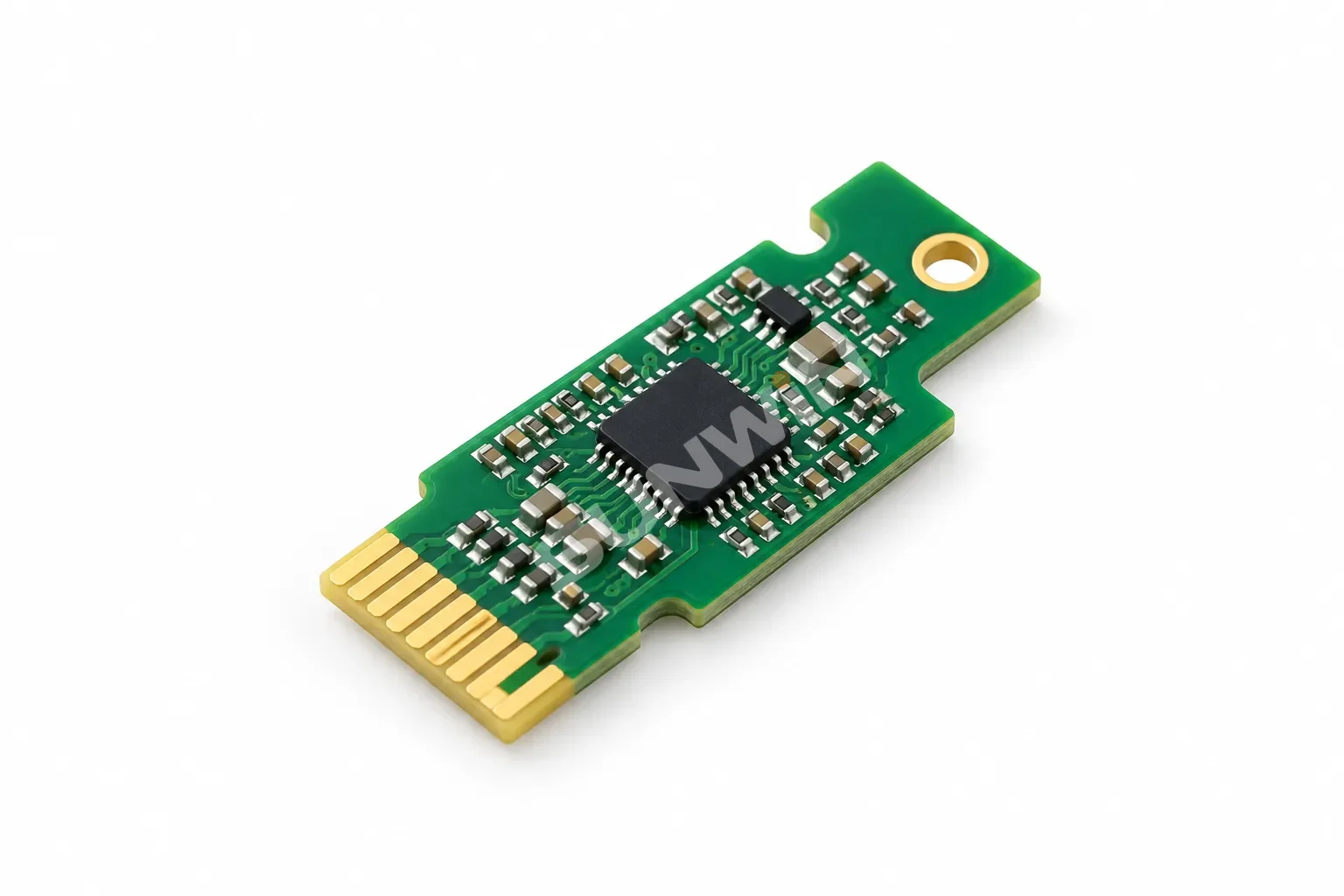
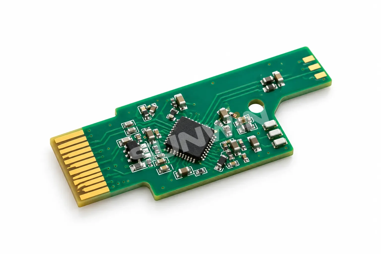
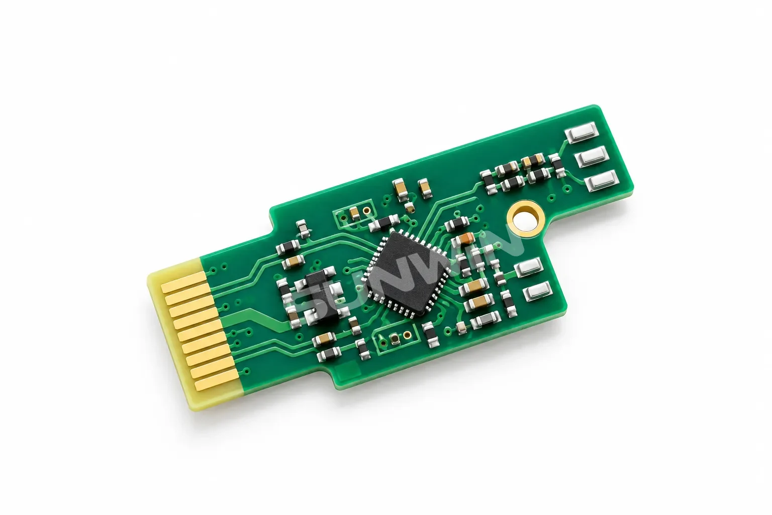
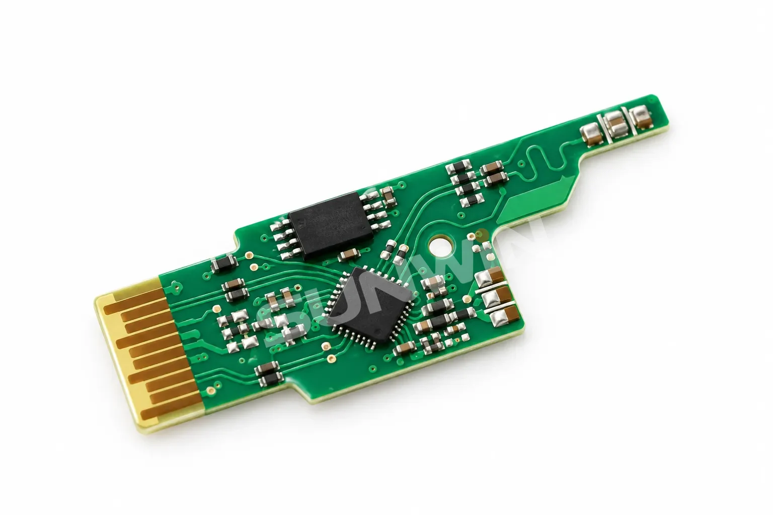
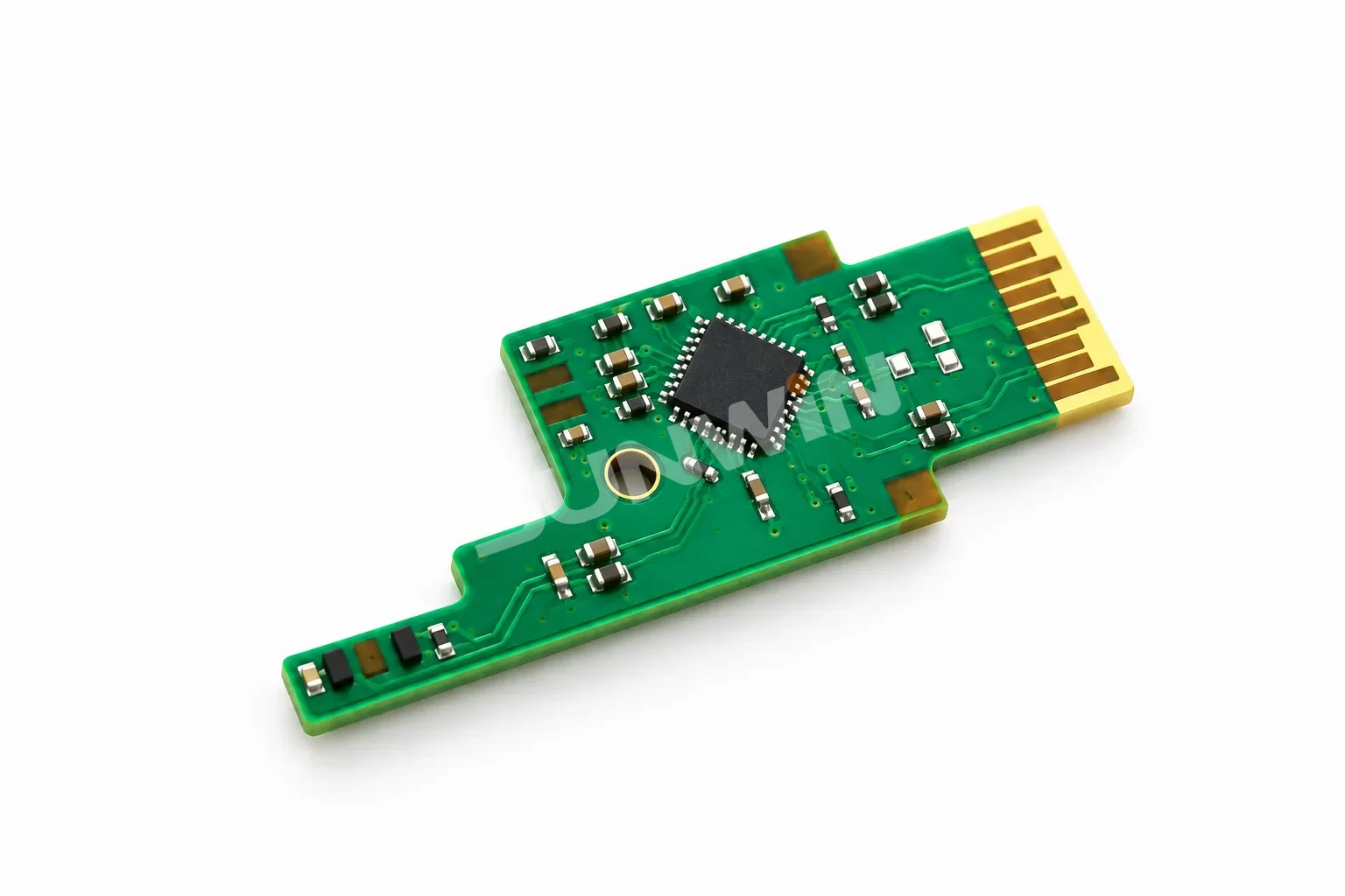
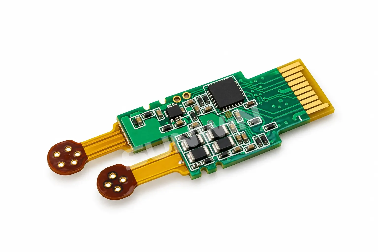
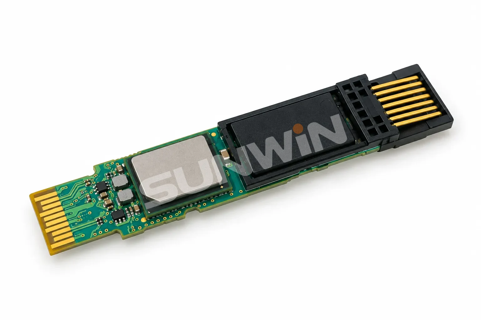
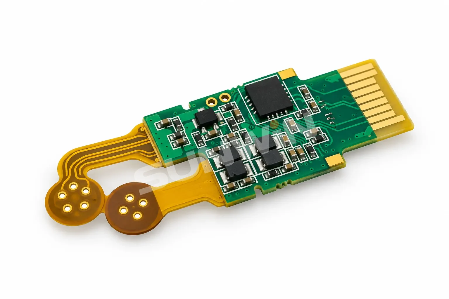
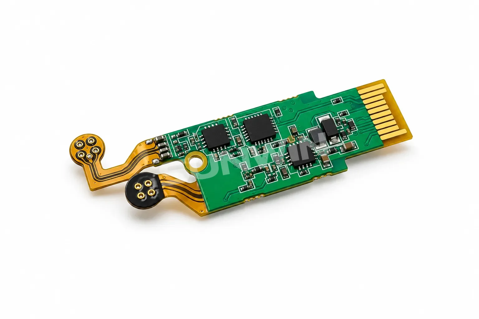
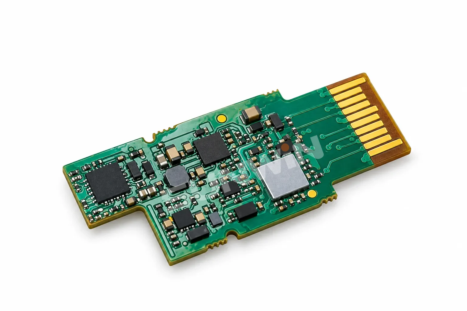
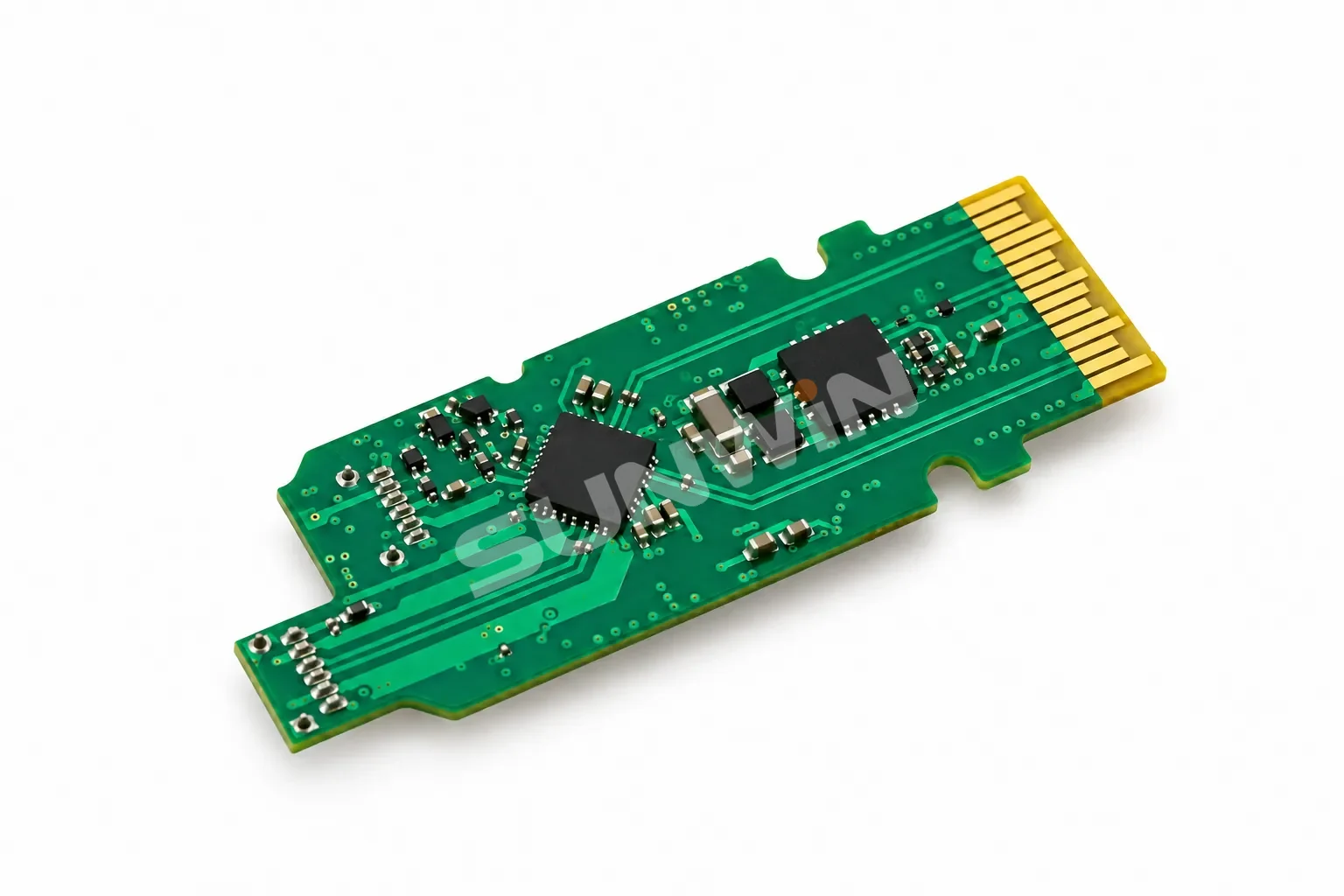
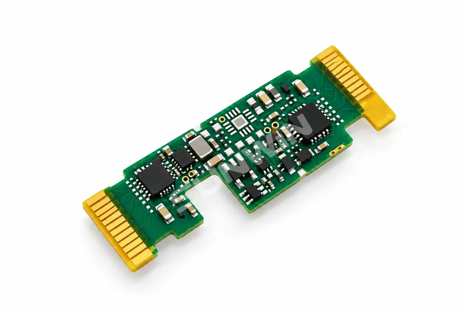
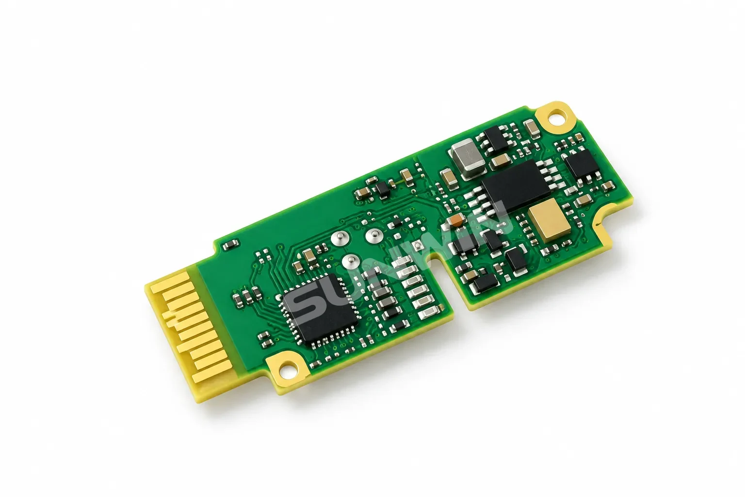
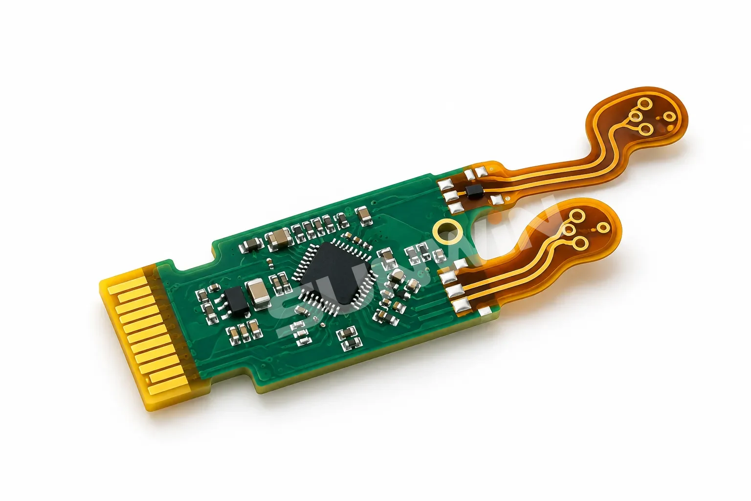
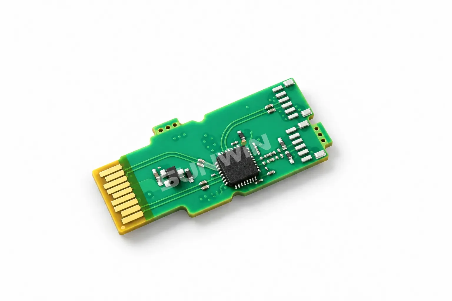
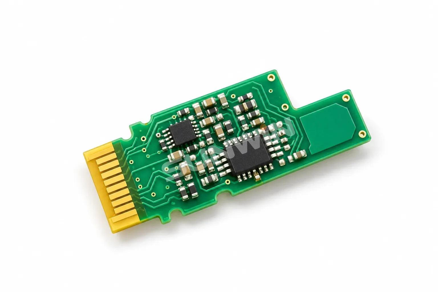
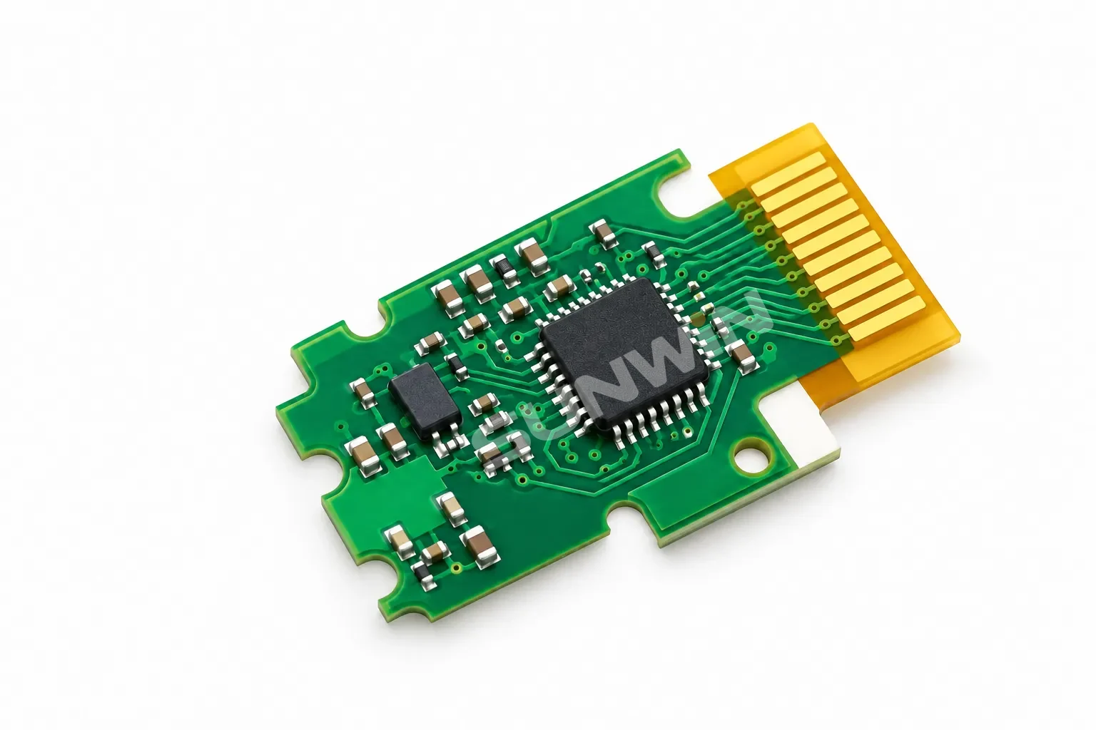
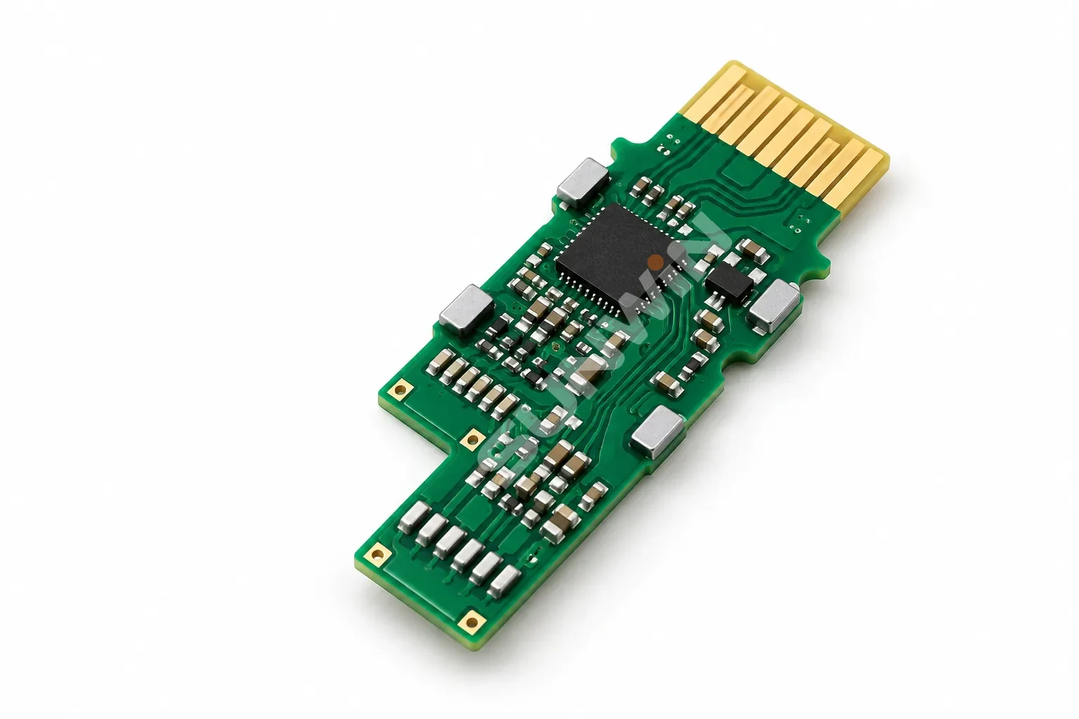
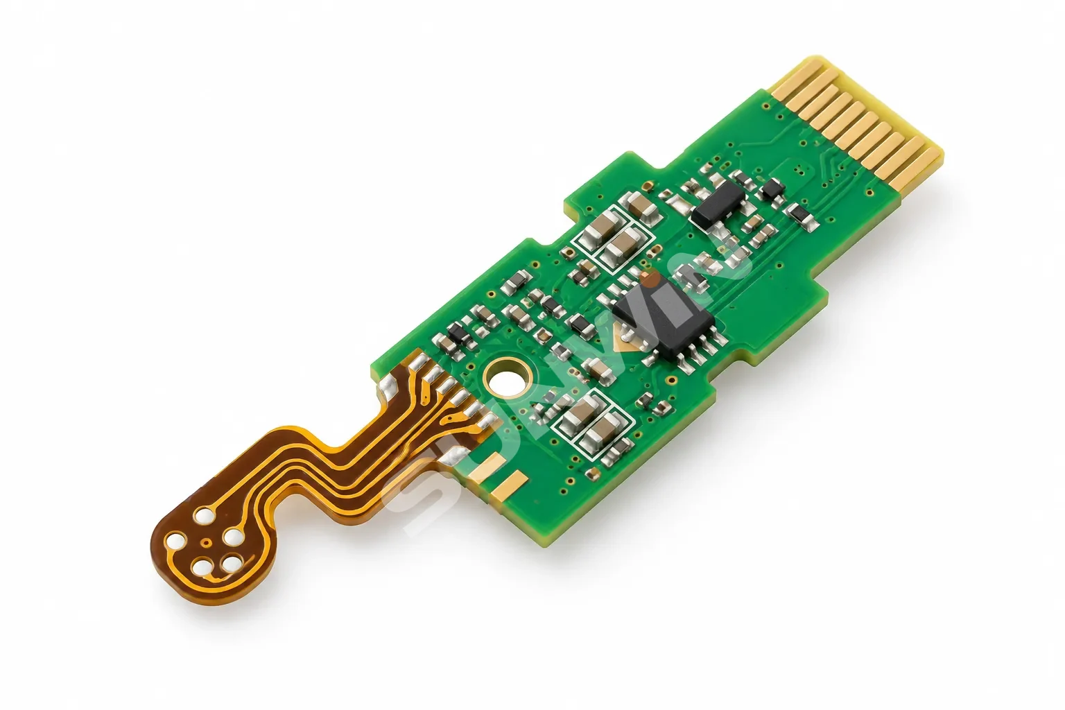
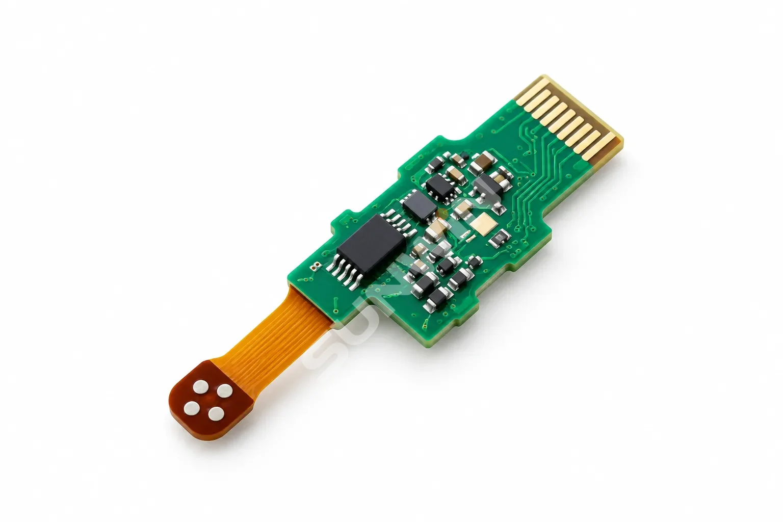
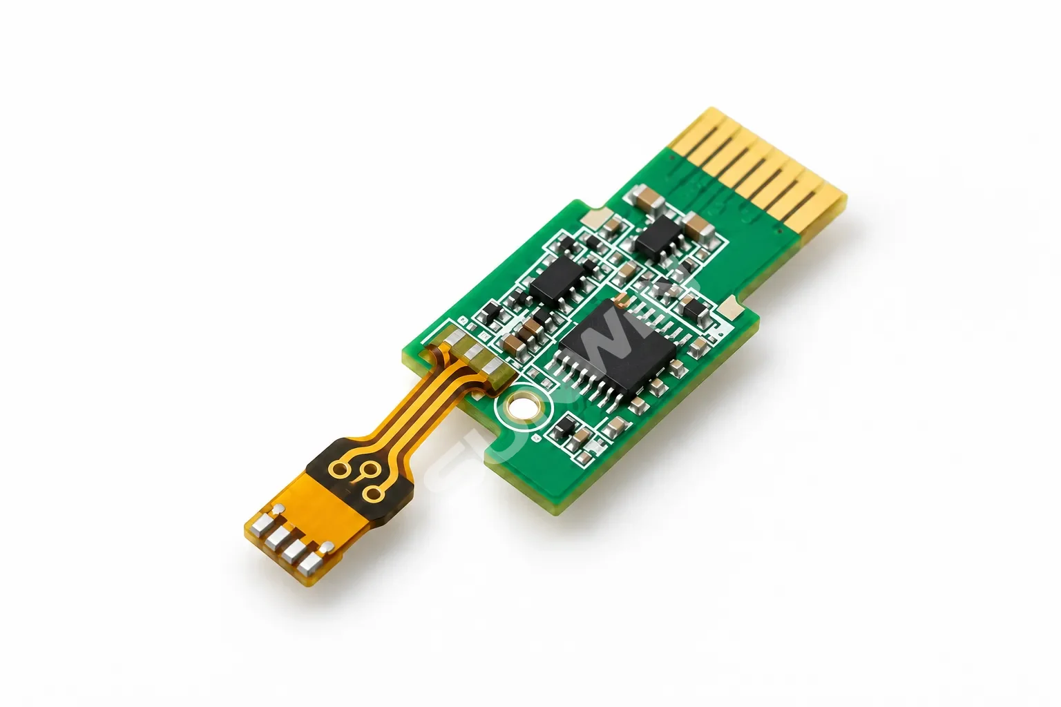
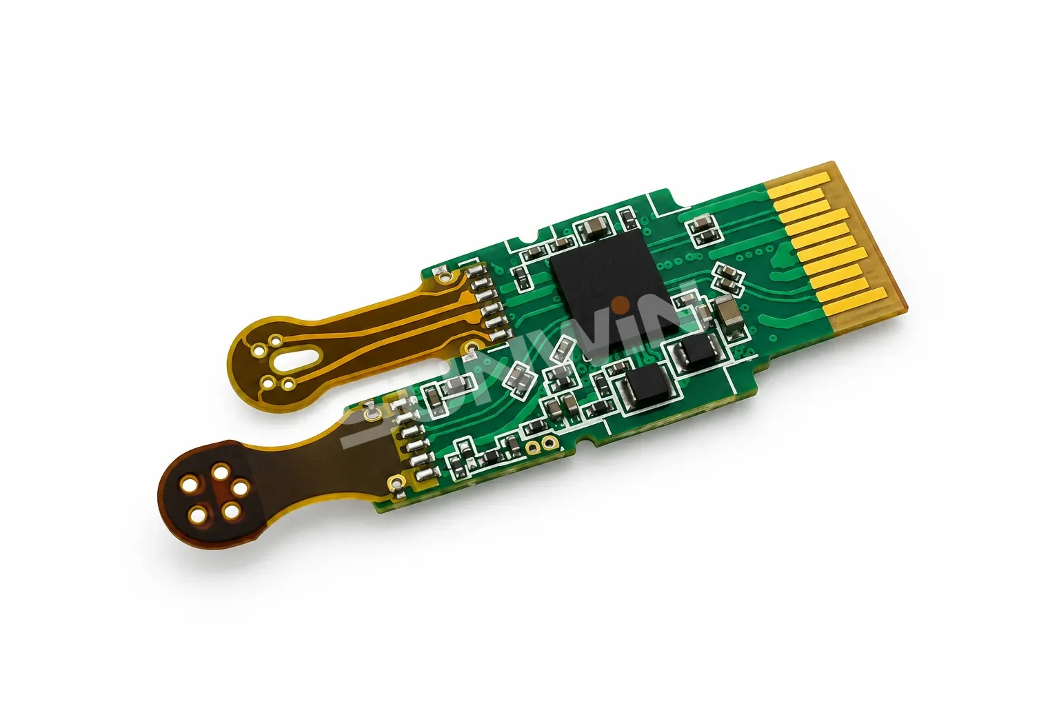
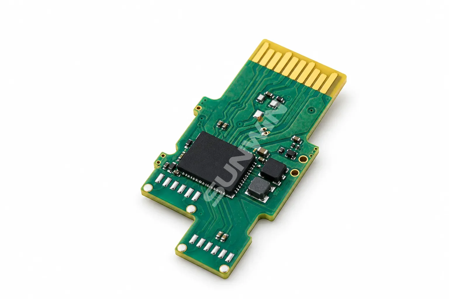
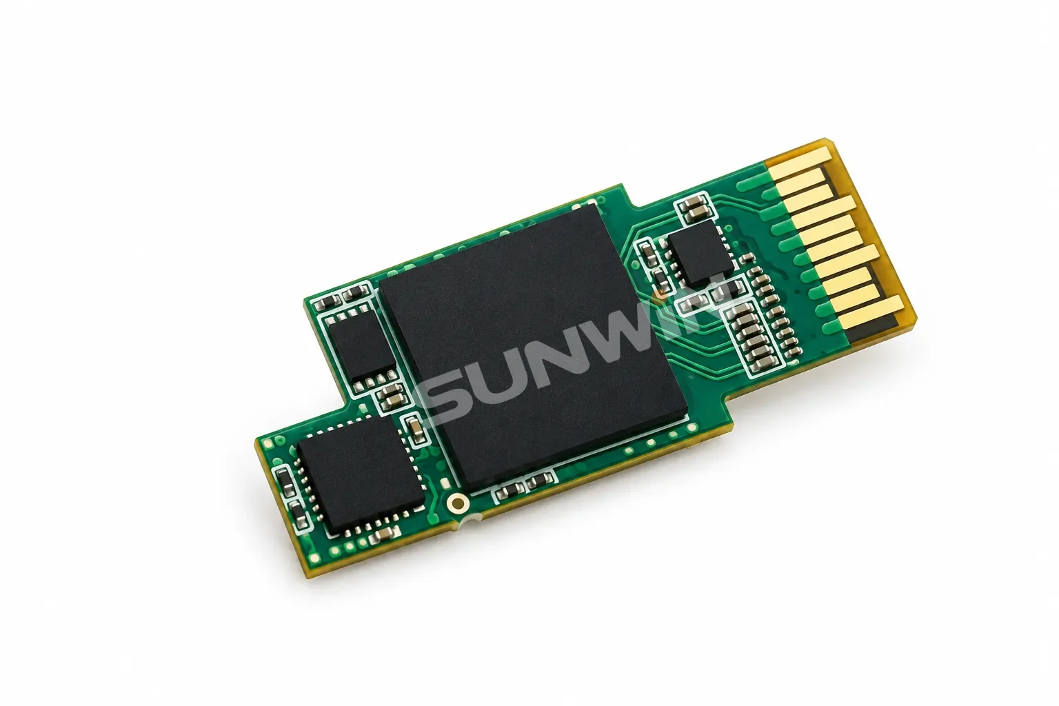
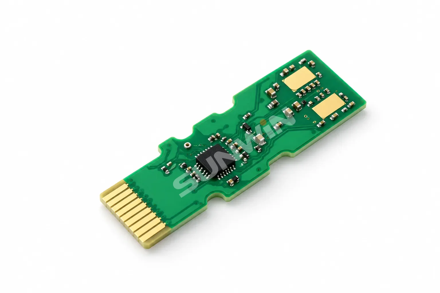
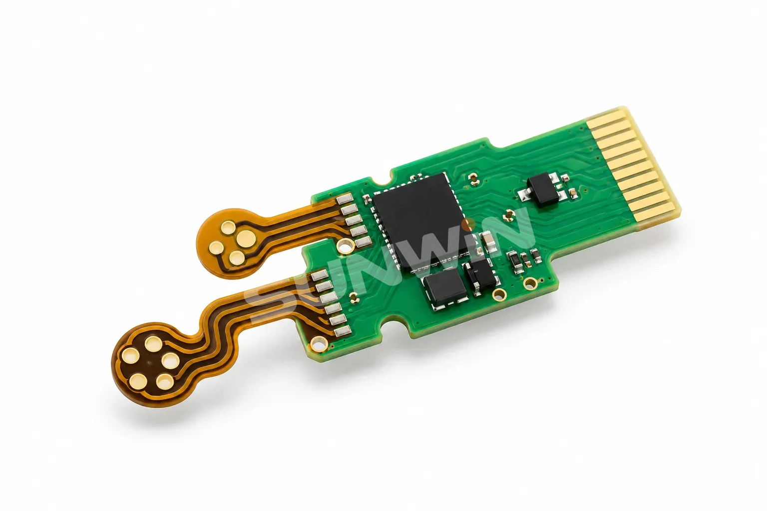
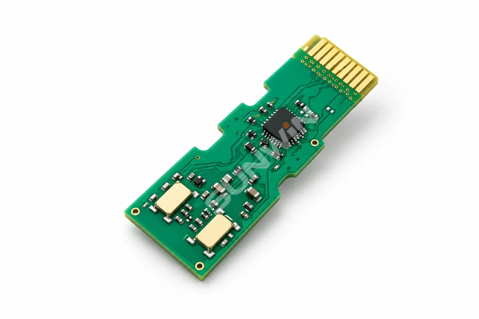
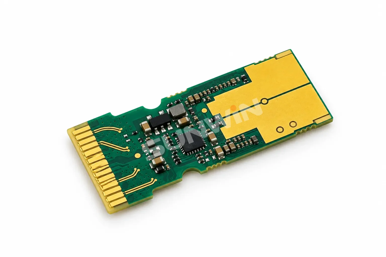
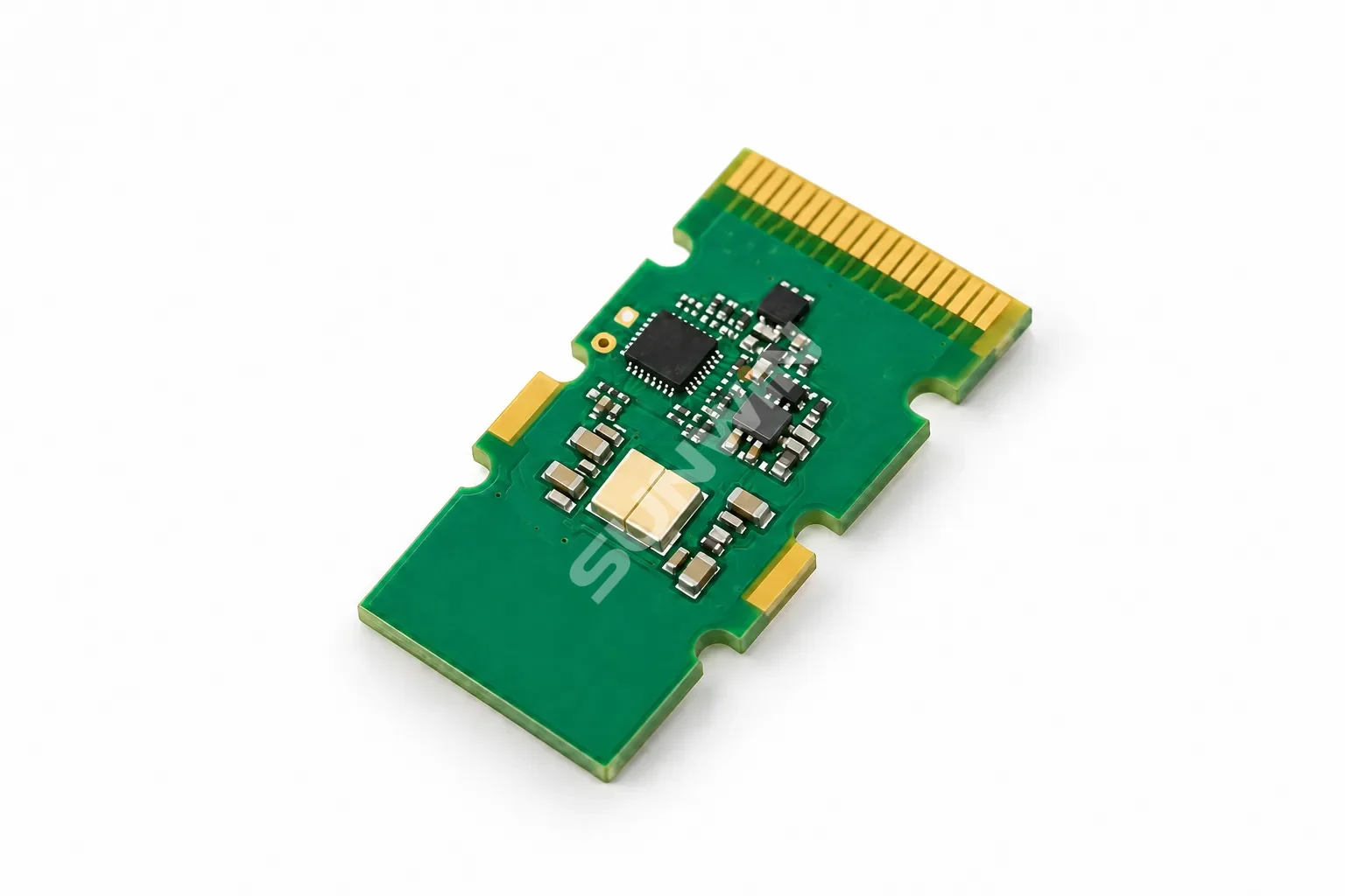
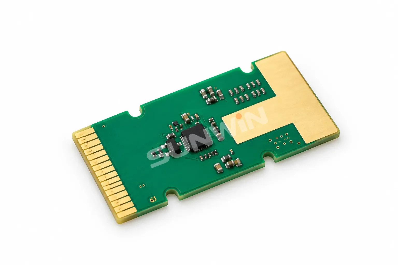
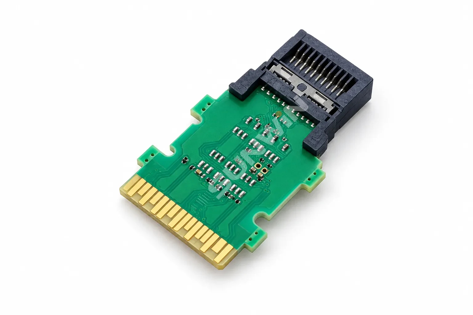
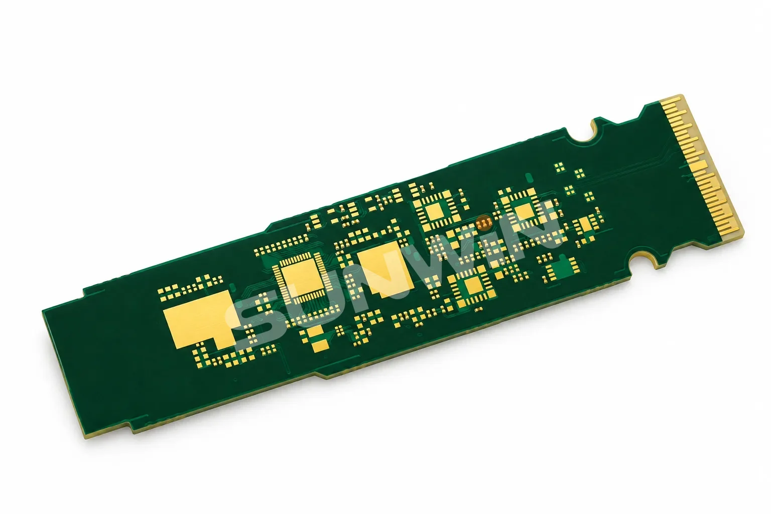
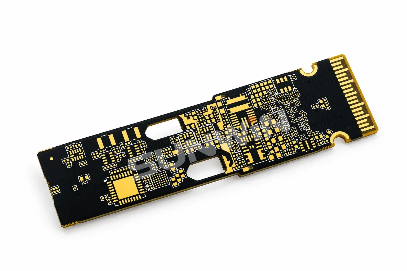
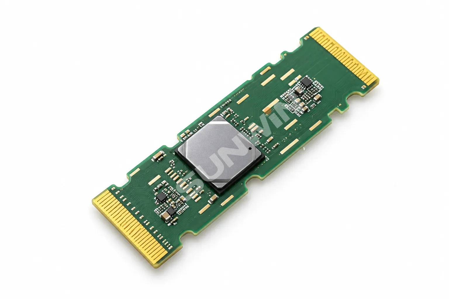
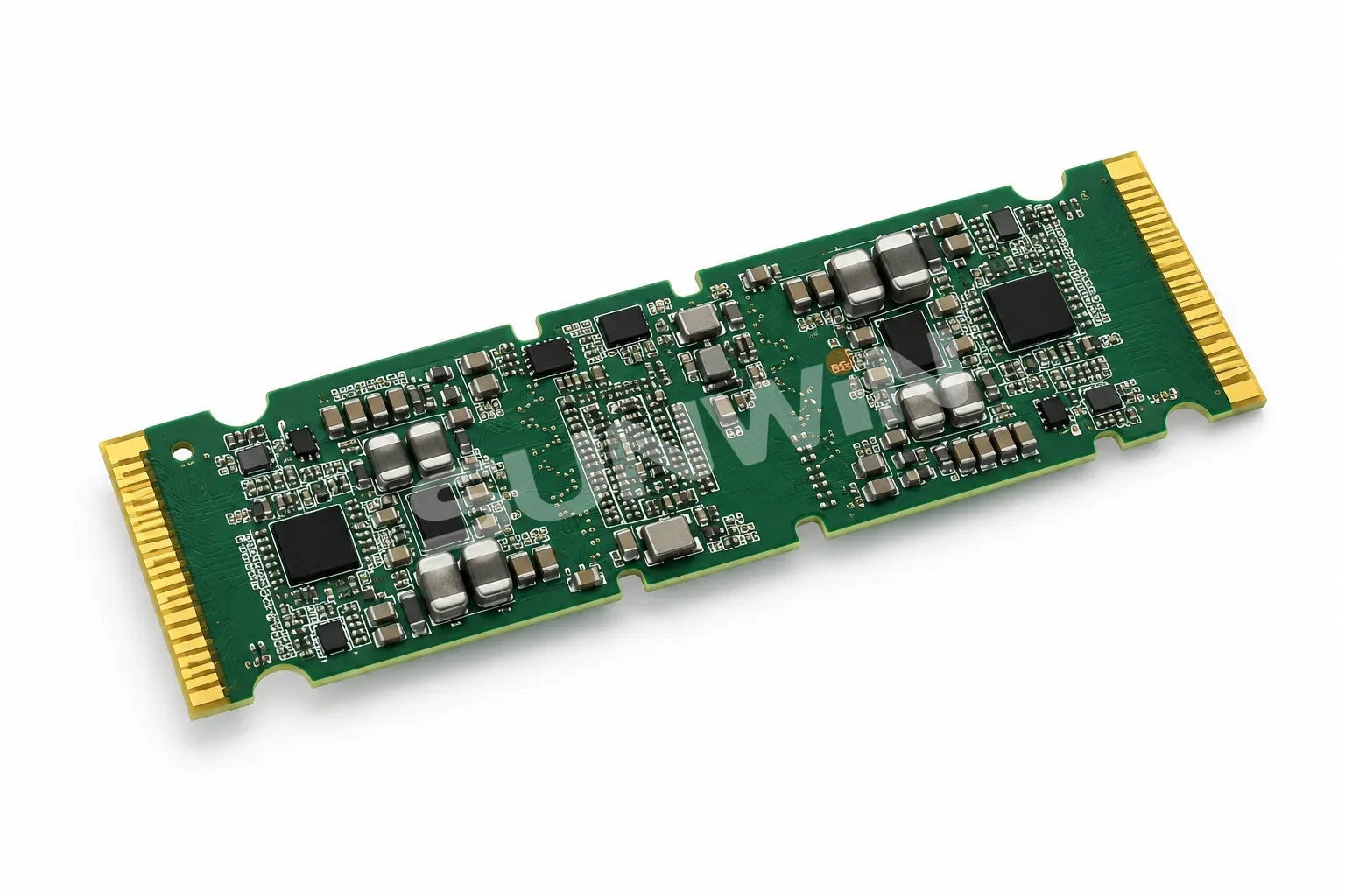
Optical transceiver PCBAs from 10G to 1.6T. Boards from 2.5G through 800G are in production, including 800G volume runs above 50,000 units.
110 μm bump pitch with a minimum bump diameter of 60 μm. Flip-chip assembly has been in volume production for multiple customers with first-pass yield above 98%.
COB and gold-finger areas are covered with high-temperature tape before printing, boards run on aluminium fixtures through nitrogen reflow, and every board receives a full 3D CCD inspection of the COB area afterwards.
To start an evaluation, send your Gerber or drawing files, BOM, package or assembly specification, test and quality requirements, and forecast volume.
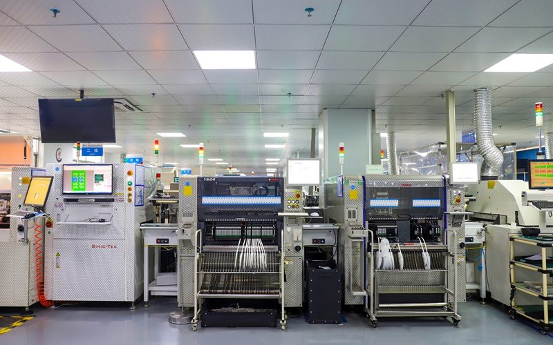
Sunwin is the overseas business company of Shenzhen Saketron Electronics Technology Co., Ltd., its shareholder and manufacturing base since 2009. 21 SMT lines · 8,000+ m². Factory certifications
To start an evaluation, send your Gerber or drawing files, BOM, package or assembly specification, test and quality requirements, and forecast volume.

Scan with WeChat to add us